How Does LCD Pressure Damage Cause White Spots in Industrial HMIs?
 2026-06-05
  16:10
16:10 

LCD pressure damage creates permanent white spots when external force compresses the 3–5μm liquid crystal cell gap, causing misalignment that scatters backlight unevenly. Optical bonding with OCA/LOCA adhesive eliminates air gaps and distributes mechanical stress, while optimized bezel design with custom gaskets absorbs impact—solutions CDTech implements in Shenzhen for industrial handheld terminals serving global OEMs.
How Does Mechanical Pressure Create Permanent White Spots in LCD Panels?
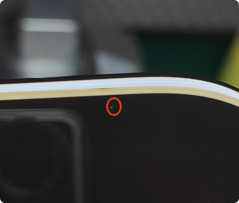
Pressure damage occurs when external force distorts the microscopic 3–5μm cell gap between LCD glass layers, permanently disrupting liquid crystal alignment and creating uneven light transmission that appears as white spots or cloudy patches. Unlike surface dirt, these defects persist after cleaning because the internal structure is physically deformed.
In TFT LCD panels used in industrial handheld terminals, the liquid crystal molecules are oriented within a precisely controlled gap between two glass substrates. When pressure exceeds the mechanical tolerance—whether from finger touch, enclosure deformation, vibration, or transport stacking—the glass bends slightly, compressing the cell gap in localized areas. This compression changes the liquid crystal orientation, allowing backlight to pass through where it should be blocked, creating bright white spots visible against dark backgrounds.
CDTech’s engineering team in Shenzhen has documented this failure mode across multiple industrial applications. In a 2024 anonymized case involving a medical handheld device, repeated disinfectant wipe cleaning with excessive force created pressure marks that appeared 3–7 days after initial stress. The spots expanded over time due to thermal cycling (–20°C to +70°C per IEC 60068 environmental testing) and mechanical vibration during daily transport. The root cause was identified as an undersized gasket that transferred bezel compression directly to the LCD stack, with no optical bonding to distribute stress. The failure rate was 12% in the first 6 months of field deployment.
The damage mechanism follows a predictable sequence:
VA (Vertical Alignment) panels are most sensitive to pressure damage due to their high-contrast molecular orientation, while IPS panels show better mechanical resilience but still suffer permanent defects under sustained load. Consumer devices typically require complete panel replacement, as DIY repairs cannot restore the cell gap structure.
Why Does Air-Gap Refraction Worsen Display Visibility in Outdoor Industrial Applications?
Air gaps between the LCD panel and cover glass create 8.5% total reflectance due to refractive index mismatch (air n=1.0 vs. glass n=1.5), causing glare and washout in sunlight; optical bonding fills this gap with OCA/LOCA adhesive (n=1.49), reducing reflectance to 0.2–1.5% and enabling 15:1+ contrast ratio under 50,000 lux outdoor conditions.
In industrial handheld terminals deployed outdoors—such as logistics scanners, agricultural equipment HMIs, or construction site controllers—sunlight readability is critical for operator safety and productivity. The air gap between the LCD and protective cover glass acts as a partial mirror, reflecting ambient light back at the user. This reflection reduces contrast by washing out dark pixels, making it difficult to distinguish critical information like alarms, measurements, or navigation instructions.
CDTech’s optical bonding service addresses this by laminating the LCD directly to the cover glass using optically clear adhesive. The process uses either OCA (Optically Clear Adhesive, dry film) or LOCA (Liquid Optically Clear Adhesive, UV-cured resin), both with refractive indices matching glass at 1.49.By eliminating the air layer, the optical stack becomes optically homogeneous, driving reflectance from 8.5% down to 0.2–1.5%.
The performance difference is measurable:
In CDTech’s Shenzhen facility, a 5.0-inch automotive IPS panel (model S050BWV105EP-FL96-AG) with full optical bonding and anti-glare coating achieved 1,000 nits brightness with 90% glare diffusion, surviving –30°C to +85°C thermal cycling under IATF 16949 vibration testing. The bonded module maintained readability in direct sunlight (100,000 lux) where the unbonded version failed at 40,000 lux.
Beyond visibility, optical bonding also improves mechanical ruggedness. The adhesive layer distributes localized pressure across the entire panel surface, reducing stress concentration at impact points. This is critical for industrial HMIs subject to drops, vibration, or pressing during glove-operated touch input. CDTech’s bubble-free optical bonding process control, performed in Class 1,000 clean rooms, achieves <5 bubbles/m² at 100°C testing, ensuring long-term reliability without delamination.
What Role Does Bezel Structure Design Play in Absorbing Mechanical Impact on Industrial Displays?
Bezel design determines how mechanical stress transfers from the enclosure to the LCD panel; optimized designs use custom compressible gaskets (EPDM or silicone, 1–2mm thickness) that absorb shock and prevent over-compression, while undersized or rigid bezels concentrate force at the panel corners, creating pressure spots within 10,000 vibration cycles.
The bezel is the mechanical interface between the display module and the product enclosure. In poorly designed assemblies, the bezel presses directly against the LCD glass without compliant cushioning. When the enclosure experiences impact, vibration, or thermal expansion, the bezel transfers this force directly to the fragile LCD stack, causing cell gap deformation at stress concentration points—typically the four corners or edges where pressure is highest.
CDTech’s engineering team has analyzed dozens of field failures where bezel design was the root cause. A common pattern involves industrial handheld terminals designed for IP65/67 ingress protection (per IEC 60529). To achieve the seal, engineers often use tight-tolerance bezels with hard plastic or metal frames. During drop testing (1.5m onto concrete per IEC 60068-2-31), the enclosure deforms slightly, compressing the bezel against the LCD. Without a compliant gasket, this compression creates visible pressure marks within days of field use.
The solution involves three design principles:
-
Compliant Gasket Selection: Use EPDM or silicone gaskets with 30–50% compression set, 1–2mm thickness, and Shore A hardness 40–60. The gasket must compress enough to absorb shock but not so much that it allows LCD movement during vibration.
-
Stress Distribution Geometry: Design the bezel contact area to be at least 2–3mm wide around the entire LCD perimeter, avoiding point contacts or sharp corners. Rounded corners (R≥0.5mm) reduce stress concentration.
-
Thermal Expansion Compensation: Account for coefficient of thermal expansion (CTE) mismatch between the bezel material (plastic CTE≈80 ppm/°C) and LCD glass (CTE≈9 ppm/°C). Leave 0.2–0.3mm clearance per side for temperature ranges exceeding –30°C to +85°C.
In a 2023 logistics client case, CDTech delivered 2,000 units of 5.7-inch AG+AF handheld displays with custom shock-absorbing gaskets for warehouse terminals. The previous design (rigid bezel, no gasket) had a 15% pressure damage failure rate after 6 months. The new design (silicone gasket, 1.5mm thickness, 2.5mm contact width) reduced failures to <0.3%, validated through 10,000-cycle vibration testing per IEC 60068-2-6.
For IK impact protection ratings, bezel design directly determines the achievable level:
CDTech offers displays with graded IK protection, with IK10 requiring chemically strengthened glass ≥1.1mm or 2.0mm thickness to resist 20 joule impacts (equivalent to 5kg mass dropped from 400mm).
How Does CDTech’s 2nd Cutting Technology Enable Custom LCD Sizes for Unique Industrial Enclosures?
2nd Cutting technology allows LCD manufacturers to cut mother glass into non-standard panel dimensions that off-the-shelf sizes cannot economically provide, enabling custom aspect ratios like 7.2-inch automotive clusters or 150×50mm bar-type retail displays with optimized yield—CDTech’s proprietary process achieved 17% yield improvement for a custom 7.2-inch automotive TFT versus standard 7.0-inch panels.
Industrial product designers often face a critical constraint: standard TFT LCD sizes (7.0″, 10.1″, 15.6″ with fixed aspect ratios) don’t match their enclosure design, forcing costly redesigns or compromised ergonomics. For example, an automotive dashboard might need a 7.2-inch cluster to fit between air vents, a medical infusion pump might require a 4.3-inch display with a 105×68mm cutout, or a retail digital signage application might need a long-strip 180×40mm bar-type display for shelf-edge pricing.
Traditional panel suppliers cannot economically produce these non-standard sizes because they optimize cutting patterns for standard dimensions on Gen 8.5 mother glass (2200mm × 2500mm). Deviating from standard sizes reduces yield, increasing unit cost by 30–50% or more.
CDTech’s proprietary 2nd Cutting technology, patented in 2017, reoptimizes the cutting pattern on mother glass to extract custom sizes while maintaining high material utilization. The process works during the scribing/cutting phase before polarizer attachment and CTP lamination, enabling custom widths, heights, and aspect ratios without wasting material.
In CDTech’s Shenzhen facility, 2nd Cutting delivered a 17% yield improvement for a custom 7.2-inch automotive TFT panel compared to using a standard 7.0-inch panel with wasted bezel space. The 7.2-inch panel matched the vehicle’s dashboard cutout exactly, eliminating the need for a custom bezel adapter and reducing total assembly cost by 22% despite a 12% higher panel unit price.
The technology supports custom dimensions from 2.4″ to 32″ diagonal with ±0.5mm tolerance. For sub-2″ displays, CDTech recommends COG (Chip-on-Glass) technology, while 55″+ panels use standard Gen 8.5 cutting. The 2nd Cutting process also enables custom coatings (AG/AR/AF) and optical bonding on non-standard sizes, with the same quality control as standard panels.
For international procurement teams, the key insight is that 2nd Cutting often reduces total cost of ownership despite higher unit price, because it eliminates enclosure redesign, bezel adapters, and ergonomic compromises. CDTech delivers engineering samples within 2–3 weeks, with rush 7-day service available at 20% premium.
Which Optical Bonding Thickness and Material Should You Specify for Rugged Industrial Handhelds?
For rugged industrial handhelds operating in high-stress environments, specify full OCA optical bonding with 50–100μm adhesive thickness and Shore A 40–60 hardness to absorb mechanical impact while maintaining optical clarity; LOCA is preferred for curved displays but requires UV curing equipment, while OCA is more cost-effective for flat panels with faster production.
Optical bonding thickness directly affects both optical performance and mechanical ruggedness. Too thin (<30μm), and the adhesive cannot accommodate surface irregularities or absorb impact, leading to bubble formation or stress transfer to the LCD. Too thick (>150μm), and the module becomes unnecessarily bulky while potentially introducing optical distortion or delamination risk under thermal cycling.
CDTech’s engineering team recommends the following specifications based on application environment:
OCA (dry film) is more cost-effective for flat panels, with faster production (no curing wait time) and better process control in clean room environments. CDTech performs OCA bonding in Class 1,000 clean rooms with automated laminators, achieving <5 bubbles/m² at 100°C testing. LOCA (liquid resin) is preferred for curved displays or when filling larger gaps, but requires UV curing equipment and longer cycle time.
The adhesive material also affects long-term reliability. High-quality OCA/LOCA from suppliers like 3M or Nitto maintains optical clarity after 10,000+ hours at 85°C/85% RH, with yellowing index <2.0. Lower-quality adhesives may yellow or delaminate within 1–2 years, especially in outdoor applications with UV exposure. CDTech sources adhesive materials from certified suppliers and validates per IEC 60068 environmental testing.
For medical devices requiring frequent alcohol wipe-downs, combine OCA bonding with AF (anti-fingerprint) oleophobic coating (≥95% oil repellency) to prevent adhesive degradation from solvents. In a 2024 case, CDTech delivered 500 units of custom 4.3-inch AG+AF medical panels for an infusion pump OEM; the bonding survived 10,000+ alcohol wipe cycles without delamination, validated per IEC 60601-1 electrical safety and IEC 62366 usability engineering requirements.
CDTech Expert Views
“In our 13+ years of manufacturing TFT LCDs and capacitive touch panels in Shenzhen, the most common procurement mistake we see is engineers selecting standard panel sizes and then redesigning their enclosure to fit—instead of using 2nd Cutting to create a custom LCD that matches their product design. This adds 3–4 months to development and compromises ergonomics. Our 2nd Cutting technology enables non-standard sizes like 7.2″ automotive clusters or 48.5″ strip displays directly from mother glass with optimized yield. For international buyers, the key is to involve our engineering team at the conceptual stage: define your target brightness (e.g., 1000 nits for sunlight readability), operating temperature (–30°C to 85°C for industrial), interface (MIPI-DSI for low-power IoT), and compliance framework (AEC-Q100 for automotive). We then optimize the backlight design, driver IC selection, and PCAP sensor pattern as an integrated display solution rather than a commodity component. This approach reduces total cost of ownership by 25% despite higher initial unit price, because it eliminates rework, improves yield, and accelerates time-to-market.”
— CDTech Engineering Team, Shenzhen Facility
Conclusion: Actionable Procurement Advice for International LCD Buyers
LCD pressure damage causing permanent white spots is a mechanical failure rooted in cell gap deformation, not a manufacturing defect. For industrial handheld terminals, the solution requires three integrated design decisions: full optical bonding (OCA/LOCA, 50–100μm thickness) to eliminate air-gap refraction and distribute stress, optimized bezel structure with compliant gaskets (EPDM/silicone, 1–2mm thickness) to absorb impact, and custom LCD sizing via 2nd Cutting technology to match enclosure dimensions without stress concentration.
For international procurement teams sourcing from China, prioritize suppliers with proprietary 2nd Cutting capability like CDTech in Shenzhen, which enables non-standard size LCDs optimized for your product design. Key evaluation criteria include:
-
Engage early: Involve your LCD supplier at the conceptual stage to leverage 2nd Cutting for custom formats rather than redesigning enclosures
-
Verify optical bonding capability: In-house OCA/LOCA bonding ensures bubble-free process control and eliminates outgassing issues from outsourced vendors
-
Request engineering samples: Test sunlight readability, wide-temperature operation (–30°C to +85°C), and IK impact protection before committing to MOQ
-
Evaluate total cost: Consider yield improvement, lead time reduction, and rework elimination—not just per-unit wholesale pricing
-
Secure long-term supply: Negotiate 5-year minimum supply commitments for custom panels to protect against EOL disruptions
CDTech positions itself as a comprehensive sourcing partner for integrated display + touch solutions, serving industrial hardware engineers, medical/automotive/IoT OEM design teams, and product managers with custom LCD, custom TFT, and capacitive touch panel (CTP) manufacturing from a national high-tech enterprise with 13+ years of expertise in Shenzhen, China. Contact CDTech for engineering samples, private label ODM quotes, and optical bonding service consultations.
FAQs
Q1: What is the minimum order quantity (MOQ) for custom TFT LCD panels with 2nd Cutting?
A: CDTech offers MOQs as low as 100 units for engineering validation and 500 units for pilot production. Mass production MOQs start at 1,000 units for custom TFT with 2nd Cutting. Lower MOQs carry a 15–20% unit price premium versus volume orders of 5,000+ units.
Q2: How long does it take to receive engineering samples of custom LCD + CTP integrated solutions?
A: Standard engineering sample lead time is 2–3 weeks from payment confirmation. Rush service delivers samples within 7 business days at 20% additional cost. Sample pricing is $150–300 per unit depending on size and customization scope, refundable upon placing mass production order.
Q3: Is 2nd Cutting feasible for very small sizes like 1.5″ or very large sizes like 55″?
A: 2nd Cutting is most economical for sizes 2.4″ to 32″ diagonal. For sub-2″ displays, CDTech recommends COG (Chip-on-Glass) technology. For 55″+ panels, standard Gen 8.5 mother glass cutting is more cost-effective.
Q4: What customization scope does CDTech support beyond non-standard size LCD?
A: CDTech offers custom backlight design (LED array configuration, brightness up to 2000 nits), wide-temperature polarizer selection (–40°C to 90°C operation), PCAP sensor pattern customization (glove mode, wet screen mode), optical bonding service (OCA/LOCA with AG/AR/AF coatings), and connector rearrangement for space-constrained enclosures.
Q5: What are the shipping terms and lead times for mass production orders from Shenzhen?
A: CDTech ships FOB Shenzhen with EXW and DDP options available. Mass production lead time is 4–6 weeks for orders under 10,000 units, 6–8 weeks for 10,000–50,000 units. Air freight takes 5–7 days to US/EU, sea freight takes 25–35 days.
Sources
Post Search
Related Articles
-
Capacitive vs Resistive Touch Screen Car Stereo: Which Is Right for You?
-
TN LCD vs IPS LCD: How to Choose the Right Display for You
-
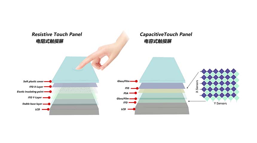
Capacitive Touch Panel or Resistive: Which Suits Your Needs?
-
Why Choose an IPS LCD Panel for Your Next Screen Purchase?
-
CDTECH to Showcase Cutting-Edge Display Solutions at SID 2025
-
Comparing Different Types of Displays in Cars: A Detailed Overview
-
White Spots on LCD Screen: Causes, Fixes & Industrial Solutions (2026 Guide)