
Is there a practical way to bridge HDMI, VGA, and Type‑C to bare MIPI/LVDS LCD panels?
 2026-07-12
  02:34
02:34 

Engineering teams can reliably bridge HDMI, VGA, DisplayPort, and Type‑C into bare MIPI/LVDS panels by using dedicated high‑speed bridge chips and LCD driver boards that perform physical layer decoding, clock recovery, color‑space conversion, and LVDS/MIPI serialization aligned to the panel’s timing and pinout. Correct EDID, power rail sequencing, and T‑Con/backlight integration are critical for stable, flicker‑free operation on custom TFT LCDs.
LCD with Driver Board Solutions
What is an embedded bridge between video interfaces and bare LCD panels?
An embedded bridge is a specialized controller board that converts standard video inputs like HDMI, VGA, Type‑C, or DisplayPort into the low‑voltage differential signaling required by raw TFT LCD panels, such as MIPI DSI or LVDS. It sits between the host SoC/PC and the bare panel, handling protocol translation, timing control, and backlight power so the system sees a “normal monitor” while the panel receives precise drive signals.
From a factory‑floor standpoint, I treat the bridge as a three‑layer device: front‑end interface, conversion core, and panel‑specific back‑end. The front‑end terminates TMDS, RGB, or AUX/CC lines; the core implements the high‑speed bridge chip with internal PLLs and color processing; the back‑end exposes LVDS or MIPI lanes, backlight boost, and sometimes touch connectors. CDTech’s custom driver boards follow this layered architecture, which makes it easier to tune each stage for EMI, jitter, and thermal behavior in real projects.
How does HDMI get converted to LVDS or MIPI for bare panels?
HDMI to LVDS/MIPI conversion relies on a bridge chip that first TMDS‑decodes the HDMI stream, recovers pixel data and clock, then re‑serializes those pixels into LVDS or MIPI DSI lanes according to the panel’s resolution, refresh rate, and bit depth. The chip typically integrates EDID handling, color space conversion, and programmable timing so the host negotiates a supported mode while the panel receives clean, panel‑native differential signals.
On the bench I always start by locking the HDMI input to a single tested resolution—say 1920×1080 @60 Hz—and verifying the TMDS eye diagram before touching the panel timing. Once the HDMI side is solid, I tune the LVDS swing voltage, common‑mode level, and mapping (JEIDA vs VESA) so the TFT LCD’s T‑Con sees correct color order and no line inversion artifacts. CDTech offers HDMI‑to‑LVDS and HDMI‑to‑MIPI boards where this mapping and drive strength are factory‑prequalified against specific TFT stacks, saving weeks of bring‑up.
How are VGA and legacy analog signals interfaced to LVDS LCD driver boards?
VGA and other analog sources feed into an ADC stage that digitizes the RGB signals and synchronizes them using HSYNC and VSYNC. Once digitized, the video is treated like a standard parallel pixel bus that the controller can scale, de‑interlace if needed, and then serialize into LVDS lanes for the LCD panel. Proper analog front‑end design, input impedance, and clamp circuitry are essential to avoid ghosting, noise, or color shift on the converted LVDS output.
In practice, I pay more attention to the analog domain than most “me‑too” guides suggest: PCB layout must keep VGA traces away from noisy DC‑DC regions, and the clamp reference needs thermal stability or the black level drifts when the enclosure warms up. On multi‑input CDTech boards that accept HDMI, VGA, and CVBS, the analog section uses guarded routing and matched impedance on the VGA pair so industrial HMI screens remain readable even under high EMI environments.
How does Type‑C and DisplayPort connect to MIPI/LVDS panels in embedded designs?
Type‑C and DisplayPort interfaces use packetized links that are converted via bridge ICs which understand DP AUX channel negotiation and USB‑C configuration channel for DisplayPort Alt‑Mode. Once a video stream is established, the bridge re‑maps the DP lanes into LVDS pairs or MIPI data/clock lanes, applying panel‑specific timing and voltage levels. This allows laptops, tablets, or SBCs with Type‑C/DP outputs to drive bare LVDS or MIPI panels through compact converter boards.
On real hardware, the most common failure is not the high‑speed PHY but Alt‑Mode negotiation: mis‑wired CC pins or incorrect pull‑up/down resistors prevent the source from entering DP mode, leaving designers chasing “no display” bugs on the panel side. I design Type‑C‑to‑LVDS boards with clearly separated CC routing and add diagnostic pads so we can confirm the correct orientation and mode during bring‑up. CDTech’s engineering team routinely validates these Type‑C paths using controlled impedance fixtures before pairing them with custom TFT LCDs.
Which physical mechanisms do high‑speed bridge chips use to translate HDMI, VGA, and DP into LVDS or MIPI?
High‑speed bridge chips from vendors such as Toshiba, Lontium, and Analogix use internal PLLs, clock‑data recovery, and protocol engines to strip framing from HDMI/DP or digitized VGA, then re‑serialize pure pixel streams into LVDS or MIPI DSI formats. Their PHY blocks implement differential drivers with controlled swing, pre‑emphasis, and skew compensation to match panel requirements, while integrated timing generators handle sync and blanking intervals for flicker‑free operation.
When I qualify a new bridge IC, I treat it like a mini‑oscilloscope experiment: measuring LVDS eye diagrams at the panel connector, checking inter‑pair skew, and verifying that spread‑spectrum clocking doesn’t violate the panel’s jitter tolerance. On MIPI, I confirm that the D‑PHY enters LP and HS states correctly during blanking; panels with tight DSI timing will show random lines or color speckle if any lane mis‑behaves. CDTech’s custom boards typically lock these parameters per project, documenting LVDS swing, MIPI lane count, and timing so OEMs can replicate results reliably.
Key bridge chip functions and signals
Why are MIPI DSI and LVDS preferred for bare TFT LCD panels?
MIPI DSI and LVDS are preferred because they efficiently carry high‑bandwidth pixel data over a small set of differential pairs while minimizing EMI, skew, and signal integrity issues. Panels are natively designed around these standards, integrating internal T‑Con logic that expects specific lane counts, voltage swings, and mapping schemes, so driving them directly via MIPI/LVDS avoids extra conversion steps and reduces latency and power consumption.
On production lines, I see LVDS dominating medium‑size industrial screens, while MIPI DSI is standard for smartphone‑class and compact high‑DPI panels. LVDS offers forgiving margins for cable length and noise, whereas MIPI excels at bandwidth density but demands stricter layout and shorter flex routes. CDTech leverages both: LVDS in large custom HMIs and MIPI in compact smart devices, choosing the interface based on panel size, resolution, and enclosure constraints rather than just matching buzzwords.
What engineering trade‑offs matter when choosing HDMI, VGA, DP, or Type‑C bridges for LVDS/MIPI panels?
Choosing the right bridge involves trade‑offs among bandwidth, latency, cabling, power, and cost. HDMI offers broad compatibility but requires TMDS decoding; DP and Type‑C add flexible resolutions and daisy‑chain options at the cost of more complex negotiation; VGA brings low cost but adds ADC noise. For panel outputs, LVDS is robust and mature, while MIPI offers superior bandwidth per lane but tighter layout requirements.
From my experience, the most overlooked trade‑off is thermal headroom: mid‑range bridge chips running multiple lanes at high data rates can exceed 90°C in tight housings, subtly increasing bit errors and reducing MTBF. I now treat heat‑spreader design and airflow as part of the interface choice; a simple LVDS‑only solution often wins over a multi‑input board if the enclosure is sealed. CDTech’s project teams model power dissipation early, adjusting copper thickness and via stitching around the bridge to keep junction temperatures in a safe range.
Typical bridge selection considerations
How does a complete LCD driver board integrate HDMI, MIPI, and LVDS for embedded systems?
A complete LCD driver board integrates multiple inputs—such as HDMI, VGA, DP, or Type‑C—with a bridge chip, T‑Con interface, backlight driver, and optional touch controller. It decodes incoming video, converts it to LVDS or MIPI, drives LED backlight with controlled PWM dimming, and exposes standard connectors that mate directly with the bare TFT LCD panel. Firmware or configuration EEPROM store panel timing, color settings, and power sequencing profiles.
When I design or evaluate such boards, I insist on three non‑negotiables: documented panel pin mapping, clearly specified backlight current limits, and repeatable power‑on/off timing. These details are where many low‑cost boards cut corners and where CDTech’s solutions differentiate. Their integrated LCD driver boards combine tested LVDS/MIPI outputs with touch and backlight management, letting OEMs focus on enclosure and UI instead of signal‑integrity debugging.
Where do Toshiba, Lontium, and other bridge IC vendors fit into embedded LCD workflows?
Bridge IC vendors like Toshiba, Lontium, Analogix, and others provide the core high‑speed chips that handle protocol decoding and LVDS/MIPI serialization. OEMs and solution providers integrate these ICs onto driver boards, adding power regulation, connectors, firmware, and mechanical design tailored to specific panels and applications. In an embedded workflow, these chips are “engines,” while companies like CDTech deliver complete “vehicles” ready for deployment.
On the line, I treat vendor reference designs as starting points, not drop‑in solutions. The reference PCB usually assumes ideal routing and a generic panel, while real devices have constrained board outlines and flex cables. Re‑spinning layouts to match enclosure and connector orientation often changes impedance enough to require re‑tuning series resistors or adding AC coupling. CDTech’s engineering advantage is their familiarity with these nuances across hundreds of panel projects, so they can pre‑select the right bridge IC and layout rules for a given use case.
Does power sequencing and backlight control affect bridge stability and panel lifetime?
Yes, power sequencing and backlight control significantly affect panel stability and lifetime. Panels typically require logic and gate driver rails to come up in a defined order before LVDS/MIPI data appears, and backlight power should be enabled only after valid video is stable. Incorrect sequencing can cause flicker, image retention, or long‑term damage to the TFT LCD. Proper PWM dimming and current control also protect LEDs from over‑drive and thermal stress.
In practical builds, I add simple hardware interlocks: the backlight enable pin depends on a “video stable” flag or a delayed power‑good signal, preventing white‑screen flashes during boot. I also derate LED current by 10–20% from datasheet maximum for devices destined for hot climates or sealed housings. CDTech’s boards typically expose configurable PWM dimming and defined power‑up timing, which lets integrators tune brightness without risking panel or backlight degradation.
Can embedded designers customize LCD bridge boards for niche resolutions and unusual mechanical sizes?
Embedded designers can absolutely customize LCD bridge boards to support niche resolutions and unusual mechanical sizes, provided they align bridge capabilities, panel timing, and PCB layout constraints. High‑speed chips often support a range of pixel clocks and lane configurations, allowing unique resolutions to be driven if the timing is within spec. Mechanical customization—such as special connector locations or second‑cut LCD sizes—requires close collaboration with the display and board manufacturer.
On factory floors I’ve seen “almost standard” panels cause months of delay because teams assumed any off‑the‑shelf board would drive them. In reality, odd resolutions or special timing (reduced blanking, custom sync polarities) need deliberate configuration. CDTech’s advanced second cutting technology and custom LCD driver boards are designed for exactly this niche: we match not only the TFT glass size but also its timing and connector geometry, ensuring that bridge IC configuration, flex routing, and mounting holes all align with the product’s industrial design.
CDTech Expert Views
“When we build a mixed‑interface LCD driver board at CDTech, I don’t start with the chip datasheet—I start with the target panel and its environment. The glass size, LVDS or MIPI timing, cable length, enclosure temperature, and EMC targets dictate whether we choose LVDS or MIPI, how we route the differential pairs, and even where we place ground stitching vias. I’ve learned that a clean eye diagram on the panel connector is worth more than any marketing spec; that’s what keeps images stable in the field and avoids returns.”
What are the key takeaways and actionable steps for interfacing HDMI, VGA, Type‑C, and DP to bare MIPI/LVDS panels?
The key takeaways are to treat the bridge as both a protocol translator and a signal‑integrity device, and to design around the panel’s native interface and environment, not just the host’s output. Actionably, teams should lock input resolutions, validate LVDS/MIPI eyes at the panel connector, implement robust power sequencing, and collaborate with display experts such as CDTech for custom boards, especially when dealing with unusual panel sizes or multi‑input requirements.
From my experience, the most effective workflow is: freeze the panel choice early, validate one “golden” video mode, then expand to other resolutions only after the LVDS/MIPI path is clean and thermally stable. Avoid chasing feature lists—multi‑input boards, rotation, and scaling are valuable, but only if the basic pixel transport is rock‑solid. Partnering with CDTech or similar specialists turns these principles into tested hardware, reducing risk for embedded teams and shortening time‑to‑market.
FAQs
What is the safest way to start bring‑up on a new HDMI‑to‑LVDS panel?
Begin with a single known‑good resolution supported by both the panel and bridge, verify LVDS mapping and voltage levels, and only then explore other modes. This minimizes variables and exposes wiring or timing errors quickly.
Are MIPI panels harder to drive than LVDS panels in embedded systems?
MIPI panels demand stricter layout, shorter cables, and more careful lane configuration, but modern bridge ICs simplify protocol handling. LVDS is more forgiving electrically, so many industrial designs still prefer LVDS for robustness.
Can I use a generic HDMI driver board for any TFT LCD panel?
Generic boards may work for common resolutions and pinouts, but panel‑specific timing, LVDS mapping, and backlight constraints often require customization. Always check panel datasheets against the board’s supported formats and power rails.
Does Type‑C Alt‑Mode always support external bare panels?
Type‑C Alt‑Mode must be correctly negotiated and wired for DisplayPort output, and then converted via a bridge to LVDS or MIPI. Not all devices expose DP Alt‑Mode or support the resolutions your panel requires, so verification is essential.
Who should I work with for custom LCD sizes and multi‑interface driver boards?
For projects combining unique LCD sizes, custom timing, and mixed inputs like HDMI, VGA, DP, and Type‑C, partnering with an experienced display specialist such as CDTech ensures proper panel selection, bridge IC choice, and robust driver board design from concept through production.
Post Search
Related Articles
-
Capacitive vs Resistive Touch Screen Car Stereo: Which Is Right for You?
-
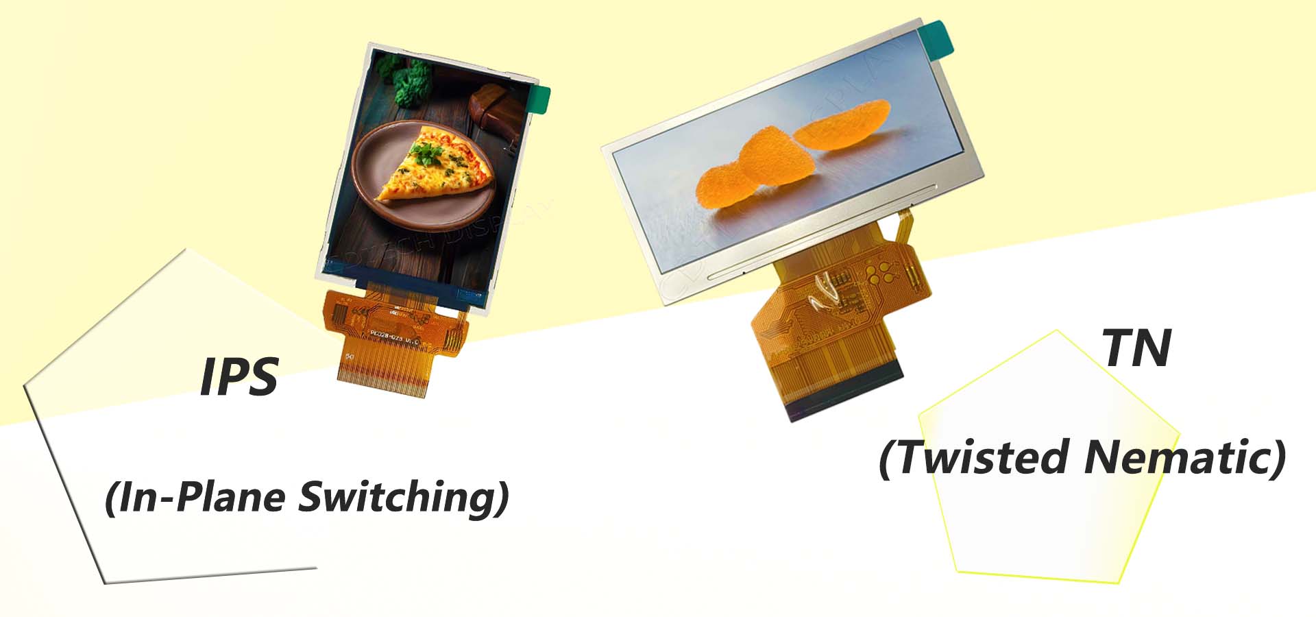
TN LCD vs IPS LCD: How to Choose the Right Display for You
-
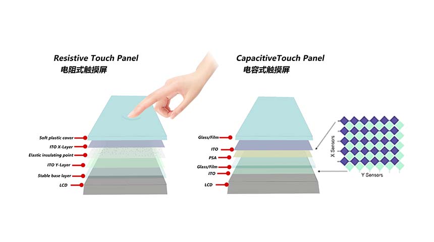
Capacitive Touch Panel or Resistive: Which Suits Your Needs?
-
Why Choose an IPS LCD Panel for Your Next Screen Purchase?
-
CDTECH to Showcase Cutting-Edge Display Solutions at SID 2025
-
Comparing Different Types of Displays in Cars: A Detailed Overview
-
White Spots on LCD Screen: Causes, Fixes & Industrial Solutions (2026 Guide)