
How can a bridge IC effectively convert RGB to LVDS for an LCD screen?
 2026-06-04
  13:13
13:13 

An LCD bridge IC, like a translator, converts incompatible video signals between a processor and a display. When your processor’s RGB output doesn’t match your screen’s LVDS input, a bridge IC solves the mismatch, enabling you to use the perfect display for your project without redesigning your entire system.
What exactly is an LCD bridge IC and how does it work?
An LCD bridge integrated circuit is a specialized chip that translates video signal formats. It acts as an intermediary, taking a digital video stream from a host processor and converting it into a format the target LCD panel can understand, effectively bridging the communication gap between mismatched components.
At its core, an LCD bridge IC performs protocol conversion and signal conditioning. It receives parallel RGB, MIPI DSI, or other interface data, then re-packages and transmits it as LVDS, MIPI, or eDP. This process involves more than simple pin mapping; the IC must manage timing synchronization, color depth translation, and often power sequencing for the panel. For instance, a common scenario involves converting a processor’s24-bit RGB output at60Hz to a single-channel LVDS stream for a high-resolution industrial panel. The bridge IC handles the clock domain crossing and ensures the pixel data arrives at the panel with precise timing, preventing artifacts like flicker or tearing. How does it manage different voltage levels between chips? It uses integrated level shifters. What about supporting various panel resolutions? It’s typically configured via an I2C interface or external EEPROM loaded with specific timing parameters. In essence, think of it as a skilled interpreter at a diplomatic summit, ensuring the intent and nuance of one language are perfectly conveyed in another. This allows engineers to mix and match components, accelerating development and leveraging existing hardware investments. Consequently, the bridge IC becomes a critical enabler for design flexibility.
How do you choose the right bridge IC for an RGB to LVDS conversion?
Selecting the correct bridge IC requires evaluating your processor’s output capabilities and your display’s input requirements. Key factors include the input and output interface types, supported resolutions and color depths, power consumption, package size, and the availability of configuration tools and support.
The first step is a meticulous specification audit. You must document your source’s output format: is it RGB with16,18, or24 bits per pixel? What is the pixel clock frequency? Then, analyze the target LVDS panel: does it use a JEIDA or VESA standard? Is it a single-channel or dual-channel LVDS interface? The bridge IC must support the voltage levels of both sides, typically3.3V for the processor interface and a lower voltage like1.8V for its core. Consider the physical space; a QFN package might be necessary for compact designs versus a larger LQFP for easier prototyping. Don’t overlook the configuration method; some chips require an external microcontroller to load firmware, while others use a simple EEPROM. For example, converting a legacy ARM9 processor’s RGB output to drive a modern10.1-inch LVDS panel in a medical device demands a bridge that can handle the specific resolution and ensure rock-solid reliability. Is the chip capable of driving the long cables often needed in kiosk applications? Does it include spread spectrum clocking to reduce EMI? Furthermore, evaluating the supplier’s documentation and sample code is crucial, as a poorly supported chip can derail a project timeline. Therefore, treat the selection process as matching a key to a very complex lock.
What are the key technical specifications to compare between bridge ICs?
Comparing bridge ICs involves scrutinizing specifications like supported input/output interfaces, maximum resolution and refresh rate, color depth support, power supply requirements, operating temperature range, and package type. These parameters directly determine compatibility and performance in your end application.
| Specification Category | IC Model A (General Purpose) | IC Model B (High-Performance) | IC Model C (Low-Power, Mobile) |
|---|---|---|---|
| Maximum Output Resolution | Supports up to1920x1200 (WUXGA) at60Hz | Supports up to3840x2160 (4K UHD) at30Hz | Supports up to1280x800 (WXGA) at60Hz |
| Key Input Interfaces | 24-bit RGB,18-bit RGB, LVDS input | 24-bit RGB, Dual-Link LVDS, MIPI DSI4-lane | 24-bit RGB,16-bit RGB, MIPI DSI2-lane |
| Key Output Interfaces | Single-Channel LVDS, Dual-Channel LVDS | Dual-Channel LVDS, eDP1.4 | Single-Channel LVDS, MIPI DSI2-lane |
| Typical Power Consumption | Approximately500mW during active operation | Approximately900mW at maximum resolution | Less than200mW with power-saving features enabled |
| Primary Application Focus | Industrial HMI, Point-of-Sale systems, Automotive clusters | Digital signage, High-end medical displays, Gaming monitors | Portable handheld devices, Battery-operated instruments, IoT displays |
What are the common pitfalls in designing with bridge ICs and how to avoid them?
Common design pitfalls include improper power sequencing, ignoring signal integrity for high-speed lines, incorrect timing parameter configuration, and inadequate heat dissipation. Avoiding these requires careful PCB layout, thorough validation of configuration data, and following the manufacturer’s reference design closely.
One of the most frequent issues stems from power sequence violations. The core voltage, I/O voltage, and panel power must often be applied in a specific order to prevent latch-up or damage. Another subtle trap is assuming the default timing parameters will work; you must generate precise timing values for your specific panel, often using a tool provided by the IC vendor, and program them into the configuration memory. Signal integrity is paramount, especially for LVDS outputs running at high speeds. This requires controlled impedance routing, keeping differential pairs tightly coupled and of equal length, and providing a solid ground plane. For instance, a designer might get a video signal but experience intermittent noise because the LVDS pairs were routed over a split plane. Have you properly terminated the lines? Is the clock signal free from excessive jitter? Additionally, thermal management is often overlooked; a bridge IC in a small enclosure without airflow can throttle or fail. Always consult the thermal resistance ratings in the datasheet. By methodically addressing these areas from the start, you can prevent frustrating debug sessions and ensure a stable, production-ready design.
Which application scenarios most urgently need an RGB to LVDS bridge?
Scenarios that urgently need conversion include upgrading legacy systems with modern displays, prototyping with development boards, integrating custom panels into standard hardware, and repairing equipment where the original display is obsolete. The bridge extends the life and functionality of existing electronic platforms.
The need for a bridge IC becomes acute in product lifecycle management. Consider industrial control systems deployed for decades; the original CRT or early TFT may fail, but the main control board remains functional. A bridge IC allows a modern, readily available LVDS LCD to serve as a drop-in replacement, saving enormous requalification costs. In prototyping, an engineer using a popular Raspberry Pi or BeagleBone board, which outputs HDMI or parallel RGB, can quickly interface with a beautiful LVDS panel meant for a final product, accelerating proof-of-concept work. Another critical scenario is in medical device repair, where original display modules are discontinued. A technician can use a bridge IC to adapt a new panel, restoring critical equipment to service. What about a startup creating a smart home device with a custom UI? They can select a cost-effective processor with RGB output and pair it with a high-quality LVDS panel using a bridge, optimizing the bill of materials. Thus, the bridge IC is a linchpin for innovation, repair, and continuity, proving that not all progress requires starting from scratch.
How does integrating a bridge IC impact overall system design and cost?
Integrating a bridge IC adds component cost and board space but saves significant development time and system-level cost. It avoids the expense of redesigning a main processor board, allows the use of optimal-cost displays, and reduces risk by simplifying the video interface portion of the design.
| Design Aspect | Impact & Consideration | Cost Implication | Mitigation Strategy |
|---|---|---|---|
| Bill of Materials (BOM) | Adds the bridge IC, configuration EEPROM, supporting passives, and possibly level shifters. | Increases direct BOM cost by $2 to $15 depending on IC performance and volume. | Offset by allowing use of a lower-cost host processor or a higher-volume, cheaper display panel. |
| PCB Complexity | Requires additional board area and layer count for routing high-speed differential pairs properly. | Increases PCB fabrication cost slightly; adds design time for rigorous layout. | Use reference layouts from the IC vendor; integrate the bridge and display connector in a dedicated section. |
| Power Supply | Needs clean, often multiple, voltage rails (e.g.,1.8V,3.3V) with proper sequencing. | May require additional LDOs or power management circuitry. | Select a bridge IC with wide voltage input ranges or integrated regulators to simplify power design. |
| Development Timeline | Reduces time spent on complex video driver software and FPGA development for signal conversion. | Saves weeks of engineering salary, a major hidden cost in custom design. | Leverage vendor-supplied configuration files and proven chip architecture to de-risk integration. |
| System Reliability | Introduces a new component that must be qualified; a well-chosen IC from a reputable supplier increases overall interface reliability. | Potential cost from field failures if a poor-quality IC is selected. | Source from established manufacturers like CDTech, which provides reliable components and technical data. |
Expert Views
In the realm of embedded display design, the bridge IC is often the unsung hero that enables innovation under constraint. The real expertise lies not just in soldering the chip onto the board, but in understanding the entire signal chain—from the processor’s timing characteristics to the panel’s power-on sequence. A successful integration demands treating the bridge as a system component, not just a simple adapter. This means investing time in simulation for signal integrity, especially for higher resolutions, and rigorously validating the design across temperature and voltage margins. The choice of bridge IC can make the difference between a product that ships on time and one stuck in endless debug cycles. Partnering with a solution provider that offers robust technical support and proven reference designs is invaluable for navigating these complexities efficiently.
Why Choose CDTech
CDTech brings over a decade of focused experience in display technology to the table, which directly informs their understanding of interface challenges. Their perspective is unique because they operate not just as a component supplier, but as a comprehensive display solution provider. This means they approach a bridge IC recommendation with knowledge of both the source processors and the destination panels, having designed and integrated countless display modules themselves. They can offer practical advice rooted in real-world applications, from industrial HMIs to portable medical devices. Choosing to engage with CDTech provides access to this applied expertise, potentially helping you avoid common pitfalls and select the most effective and cost-efficient conversion path for your specific project requirements.
How to Start
Begin by clearly defining your input and output signal parameters in a specification document. Gather the datasheets for your host processor’s video output and your desired LCD panel. Identify the exact interface types, voltage levels, and timing requirements. Next, research bridge ICs that fit this electrical and protocol gap, using comparison tables like the one provided earlier as a starting point. Once you have a shortlist, procure evaluation boards or modules to test the conversion in your actual environment. This hands-on testing is crucial to validate compatibility and performance. Finally, engage with the technical support team of your chosen supplier to review your schematic and layout before committing to a PCB spin, ensuring a smooth transition from prototype to production.
FAQs
Can a bridge IC convert HDMI to LVDS?
Yes, but it typically requires a two-stage process. A dedicated HDMI receiver chip first decodes the HDMI signal into a parallel RGB or other format, which is then fed into an RGB-to-LVDS bridge IC. Some highly integrated chips combine both functions, but for most designs, using two specialized chips is the standard and reliable approach.
Does using a bridge IC introduce noticeable video latency?
The latency introduced by a well-designed bridge IC is typically negligible for most applications, often in the range of a single scan line or less. This is because the conversion is a real-time, line-by-line process with minimal buffering. It is generally not perceptible in human-machine interfaces, industrial controls, or video playback. Only in ultra-high-speed, real-time graphics rendering for gaming or specialized simulation would this micro-latency potentially need consideration.
How do I program the configuration EEPROM for my bridge IC?
Most bridge IC vendors provide a configuration tool or software that generates a binary file based on your panel’s timing parameters. This file is then written to a serial EEPROM (like a24C02) using a common programmer. The EEPROM is connected to the bridge IC’s I2C configuration pins. On power-up, the bridge IC reads this data to configure itself automatically for your specific display.
Are there bridge ICs that support touch screen interfaces as well?
Yes, some advanced bridge ICs integrate a touch controller, commonly for resistive or capacitive touch screens, alongside the video conversion circuitry. This allows you to manage both the display and touch input through a single chip, simplifying system design and reducing component count. However, for complex multi-touch or very large touch screens, a dedicated touch controller is often still preferred for optimal performance.
Successfully implementing an LCD bridge IC hinges on meticulous planning and a deep understanding of your system’s video requirements. The key takeaway is that these components are powerful enablers, offering a pragmatic path to leveraging ideal displays without the burden of a full system redesign. By carefully selecting the right IC, paying close attention to power sequencing and PCB layout, and thoroughly validating the configuration, you can achieve a robust and reliable display interface. Remember to view the bridge IC as an integral part of your signal chain, deserving of the same design rigor as your processor or panel. This approach ensures your final product delivers a crisp, stable visual experience, seamlessly connecting your innovative ideas to the perfect screen.
Post Search
Related Articles
-
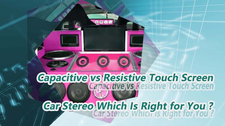
Capacitive vs Resistive Touch Screen Car Stereo: Which Is Right for You?
-
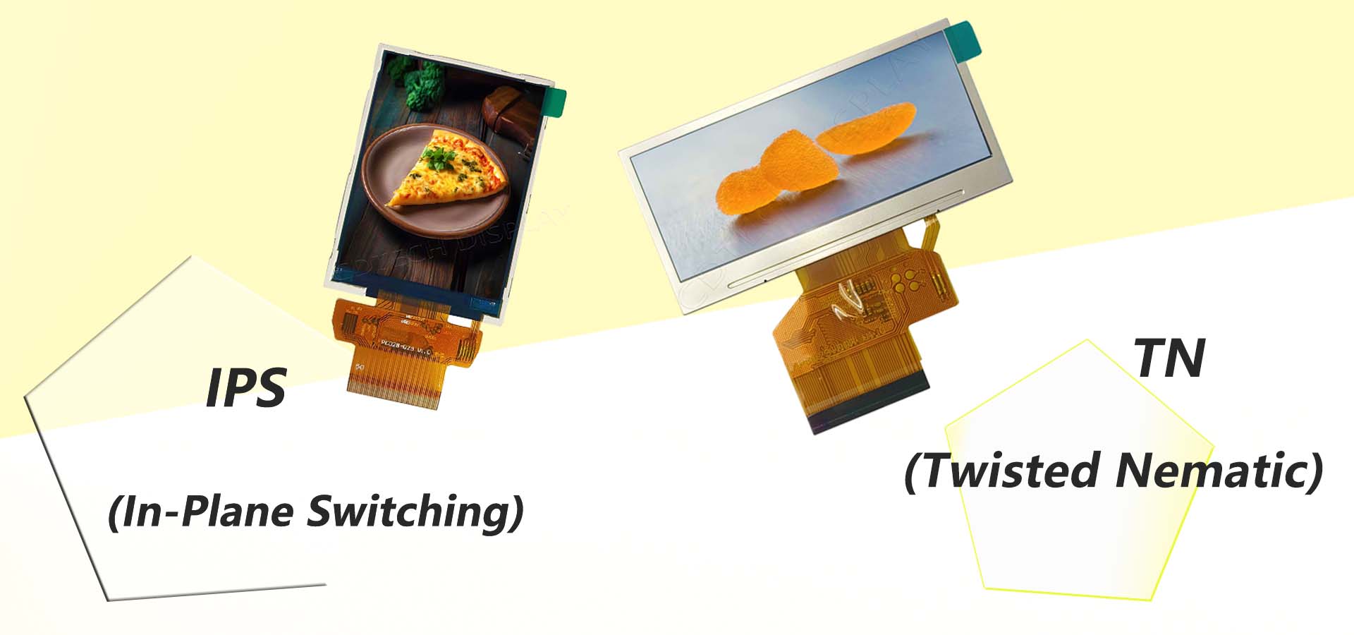
TN LCD vs IPS LCD: How to Choose the Right Display for You
-
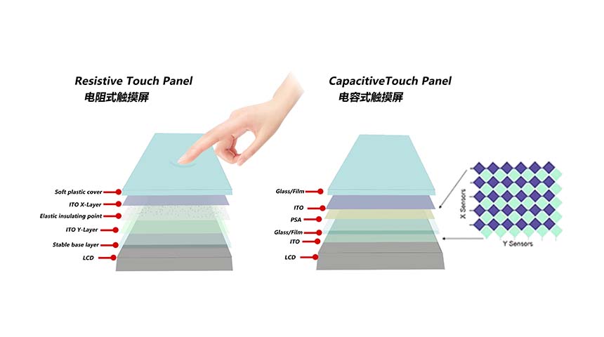
Capacitive Touch Panel or Resistive: Which Suits Your Needs?
-
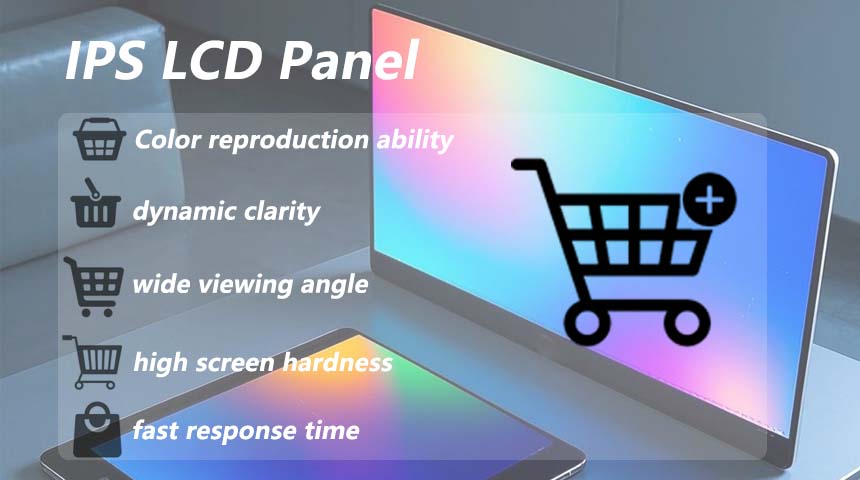
Why Choose an IPS LCD Panel for Your Next Screen Purchase?
-
CDTECH to Showcase Cutting-Edge Display Solutions at SID 2025
-
Comparing Different Types of Displays in Cars: A Detailed Overview
-

White Spots on LCD Screen: Causes, Fixes & Industrial Solutions (2026 Guide)