
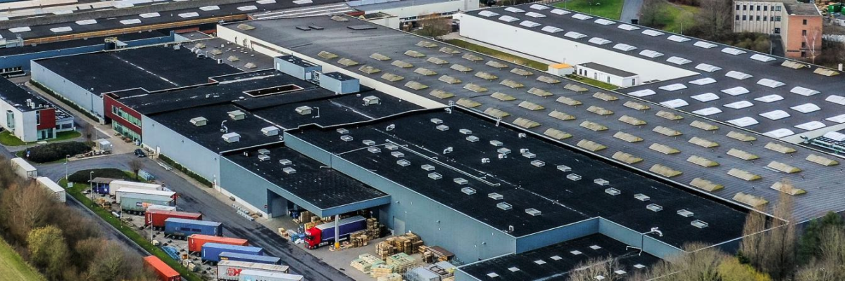
How can industrial display boards achieve robust EMC in harsh factory environments?
 2026-07-15
  02:53
02:53 

Industrial display boards achieve robust EMC in harsh factory environments by combining layered PCB grounding, controlled differential routing, and targeted shielding of radiated and conducted noise sources. By co-designing LCD driver boards with EMI filters, split ground planes and disciplined layout, CDTech ensures CE/FCC compliance and CISPR 22 performance even beside servo drives, high-frequency inverters and noisy industrial power rails.
Industrial-Grade LCD Controller Boards
What is EMC for heavy-industrial display boards and why does it matter near servo drives and inverters?
EMC for heavy-industrial display boards means ensuring the LCD controller and driver PCB neither radiate excessive EMI nor succumb to conducted and radiated noise from motors and inverters, while still meeting CE/FCC and CISPR 22 limits. In motor-packed factories, poorly hardened boards exhibit flicker, communication dropouts, ghost touches or complete resets when nearby drives ramp up or brake.
From my hands-on debugging, the worst offenders are long unshielded LVDS/MIPI lines, poorly terminated backlight driver loops and floating grounds that turn display boards into antennas. When a 30 kW inverter switches at several kilohertz, it dumps broadband noise across cabling and chassis; if the display PCB lacks solid reference planes and filtering, its logic thresholds wobble and RF energy escapes as radiated emissions. CDTech’s industrial boards are engineered from the outset for these environments, not retrofitted later with ad hoc ferrites.
Robust EMC translates into uptime: operators must be able to read alarms and setpoints even as servo motors accelerate or emergency stops are triggered. By validating driver boards in chambers with injected noise and near real equipment, we ensure that EMC is not just a lab certificate but a field-proven property that protects both the human–machine interface and the surrounding control ecosystem.
How do four-layer and six-layer PCB stacks harden EMI and EMC for industrial display driver boards?
Four-layer and six-layer PCB stacks provide dedicated planes and controlled impedance routes that dramatically reduce loop areas, common-mode emissions and susceptibility to external fields. In a four-layer stack, I typically allocate top and bottom for signals, with solid internal layers for ground and power, forming tight capacitive coupling between reference planes. Six-layer designs add extra ground or split-power planes, enabling more complex zoning and shielding.
In CDTech’s industrial driver boards, the core EMC strategy is to keep high-speed LCD interfaces and noisy switching regulators referenced tightly to continuous ground planes, never fragmented by careless splits. By stacking ground close to signal layers, we shrink return paths and minimize differential-mode radiation. On the factory floor, I’ve watched identical schematics behave completely differently simply because one used a proper four-layer stack and the other a cheap two-layer board.
Layer selection also affects routing freedom: six-layer boards allow us to route sensitive differential pairs on inner layers sandwiched between grounds, creating quasi-coaxial environments that shield them from external noise. This is especially important for LVDS, MIPI and Ethernet on display controller boards. For harsh environments with dense motor cabling, I often recommend bumping from four to six layers not for “feature” reasons but purely to gain EMC margin.
What layout techniques for split ground planes, return paths and zoning improve EMI performance on LCD controller boards?
Split ground planes are powerful but dangerous: done correctly, they isolate noisy digital sections from sensitive analog or RF zones; done poorly, they create radiating slots and unpredictable return paths. My rule in industrial display boards is to maintain a single main ground reference, then use carefully planned cuts and stitching capacitors to guide high-frequency currents without allowing them to roam across sensitive regions. CDTech’s layouts treat ground like a highway system, not random islands.
Critical techniques include: keeping high-speed digital ground continuous under LVDS/MIPI pairs, reserving separate local planes under switching regulators, and providing controlled bridges where currents must cross. I avoid long, narrow ground “necks” that behave like inductors; instead, we use broad connections and multiple vias to keep impedance low. When we must split, such as separating chassis ground from signal ground for safety and EMC, we define clear connection points and include common-mode chokes on interfaces.
On the factory floor, misrouted returns are a hidden cause of intermittent failures. I’ve seen boards pass EMC in the lab but fail near real servo drives because last-minute layout changes forced LVDS returns to cross analog ADC regions. In CDTech designs, we lock zoning early: backlight power, logic core, interface connectors and touch sense regions each get defined territories, with disciplined routing corridors and via fences to keep their noise where it belongs.
Typical EMC zoning on an industrial LCD driver PCB
How do differential pair routing and length matching reduce signal noise and radiated emissions in display boards?
Differential pair routing and length matching are more than signal integrity buzzwords; they directly impact radiated emissions and susceptibility. Balanced differential pairs cancel common-mode noise by design, but that cancellation only works when pairs are tightly coupled, matched in length and referenced to stable ground. On industrial LCD boards, I route LVDS and MIPI pairs side-by-side with consistent spacing, avoiding stubs and sharp corners that create impedance discontinuities.
Length matching ensures that each pair’s signals arrive synchronously, preventing skew that converts differential energy into common-mode radiation. The practical target is usually within tens of mils, depending on data rates, but more importantly, we keep all related pairs in a bundle with similar environments. CDTech’s controller boards place connectors, driver ICs and terminations to allow natural, clean routes; when I see “spaghetti” differential routing, I know EMC margins are already compromised.
In noisy factory halls, differential pairs also face external fields and crosstalk from power cables. By routing them on inner layers sandwiched between grounds, and by including proper terminations and sometimes common-mode chokes near connectors, we both contain their emissions and make them resilient to external noise pulses. Real-world testing near servo cabinets has shown that such hardened differential routing dramatically reduces display flicker and random bit errors under heavy load changes.
Which filtering, shielding and termination components are most effective for CE/FCC and CISPR 22 compliance in industrial LCD boards?
For CE/FCC and CISPR 22 compliance, component-level filtering and shielding complement layout design. At power entry, I use common-mode chokes, LC filters and TVS diodes tuned to expected noise spectra and surge levels. For backlight drivers and switching regulators, snubber networks and RC damping reduce ringing that otherwise radiates across the board. CDTech’s standard industrial driver board platforms integrate these blocks so OEMs start from a hardened baseline rather than bare regulators.
On signal interfaces, ferrite beads and common-mode chokes tame high-frequency noise riding on LVDS, RGB, USB or RS-485 lines. Proper terminations—series resistors close to drivers, parallel terminations at receivers—control reflections and prevent standing waves that increase emissions. In my experience, a single mislocated termination resistor can move a board from passing to failing radiated tests, especially at harmonics of pixel clocks.
Shielding complements filters. Metal or conductive plastic shields over noisy DC/DC zones, bonded to ground via multiple low-inductance vias, confine near fields. Where mechanical shields aren’t possible, we use ground pour “tents,” stitching vias and sometimes shielded FPCs to block noise from escaping through flex connections to the LCD. CDTech’s EMI-shielded FPCs, combined with board-level filtering, have proven especially effective in compact HMI units mounted directly on motor housings.
Typical EMI/EMC components used on industrial display boards
Why does CDTech invest in EMC-hardened display boards instead of relying on enclosure-level shielding alone?
Relying solely on enclosure-level shielding is tempting but dangerous: it often hides fundamental PCB weaknesses that resurface when cables, windows or apertures compromise the shield. CDTech invests in EMC-hardened display boards because fixing EMC at the board level is more reliable, scalable and cost-effective than treating the enclosure as the only defense. I’ve seen “shielded” boxes fail EMC simply because their internal boards radiated through unavoidable gaps.
Board-level hardening also improves system robustness in real factories, where operators open doors, route cables differently or add third-party modules. When the LCD driver board itself has strong EMI immunity and low emissions, the entire HMI system tolerates such variations without unexpected glitches. CDTech’s experience across thousands of deployments shows that customers who prioritize EMC in the PCB design see fewer field issues and faster certification cycles.
Additionally, board-level EMC enables more flexible mechanical designs: thinner bezels, larger display windows and lightweight plastics become feasible because the electronics do not require an “iron cage” to behave. This aligns with modern industrial aesthetics and ergonomic demands. For OEMs, partnering with a display vendor that designs EMC in from the start reduces project risk and accelerates time-to-market.
Who in the engineering chain must take ownership of EMI/EMC performance for industrial display systems?
EMI/EMC performance is a shared responsibility, but someone must own it. In successful projects I’ve led, a dedicated EMC engineer or lead system designer coordinates PCB layout, cabling, enclosure and grounding strategies, while display vendors like CDTech provide hardened board platforms and detailed application notes. Without clear ownership, EMC becomes a last-minute test result, not a design parameter.
PCB designers must understand EMC implications of routing and component placement, not just meet connectivity requirements. Mechanical engineers must consider enclosure shielding, vent placement and cable routing to avoid forming unintended antennas. System integrators must manage grounding schemes and avoid mixing safety, chassis and signal grounds without a plan. CDTech supports this chain by offering reference designs, EMC guidelines and pre-tested driver boards tailored to industrial environments.
Ultimately, OEMs that treat EMC as a core performance metric—on par with resolution and brightness—achieve more reliable systems. By formalizing EMC ownership and involving CDTech early, they can turn regulatory compliance from a stressful hurdle into a predictable design milestone backed by lab data and field experience.
CDTech Expert Views
In our heaviest industrial projects, the biggest EMC gains came not from adding more ferrites but from cleaning up return paths and ground splits. Once we aligned the board’s reference planes with the enclosure and cable strategy, CE and FCC tests went from “trial and error” to repeatable success. That’s why every CDTech driver board layout starts with an EMC plan, not just a schematic.
How does CDTech validate EMC performance of industrial LCD driver boards for CE, FCC and CISPR 22?
CDTech validates EMC performance through a structured process: pre-layout simulation, internal chamber testing and external certification. We begin by modeling critical loops, interfaces and ground configurations, then design PCBs with EMC in mind. Early prototypes undergo radiated and conducted emission tests, immunity checks and ESD stress in our labs, close to CISPR 22 and regional standards used for CE and FCC approvals.
When issues appear, we adjust layout and filter networks rather than relying on patch fixes. I’ve spent nights in chambers tweaking snubber values and re-routing differential pairs, but the outcome is driver boards that pass formal labs with minimal rework. CDTech’s engineering team documents these learnings into design rules and reference layouts, which customers can reuse across product families.
Finally, we support OEMs during formal CE and FCC campaigns, providing test histories, modification recommendations and, when needed, on-site assistance. This partnership approach shortens certification cycles and gives customers confidence that their HMI systems will meet regulatory requirements not just once but consistently across batches and variants.
When should OEMs move from basic EMC “checklist” design to full layout hardening for industrial display boards?
OEMs should move from basic EMC checklist design to full layout hardening when their displays operate near high-power drives, inverters or distributed control networks, or when CE/FCC failures have already occurred. If your HMI will live in a servo cabinet, on a robot cell, or within a noisy plant power distribution area, checklist-level EMC is insufficient; board-level hardening becomes mandatory.
Another trigger is functional instability in prototypes: flicker during motor starts, touch false triggers under ESD, or communication errors when long cables are connected. These symptoms indicate that noise margins are thin and that layout-level fixes will be more effective than ad hoc shielding. CDTech often helps customers at this stage, analyzing their existing boards and proposing hardened replacements or redesigns.
The decision is also strategic: investing in EMC layout hardening early yields reusable platforms and reference designs that support future products with minimal additional effort. OEMs who treat EMC as a one-time certification problem tend to pay more over time in redesigns and field fixes than those who embed EMC thinking into their display architecture from the start.
Conclusion: How can OEMs systematically harden display boards against EMI while maintaining performance and readability?
OEMs can systematically harden display boards against EMI by treating EMC as an integrated design discipline across PCB stack-up, layout, filtering, shielding and system grounding. Choosing four- or six-layer stacks with solid ground planes, disciplined differential routing and well-planned zoning forms the foundation. Adding targeted filters, shielded FPCs and mechanical shields then refines performance for CE/FCC and CISPR 22 compliance, even in servo-dense factories.
Partnering with a specialist like CDTech brings hardened driver boards, EMI-aware display modules and practical guidelines derived from hundreds of real industrial deployments. Actionably, define EMC requirements early, assign ownership, and validate prototypes in realistic noise environments—not just in clean labs. When EMC is designed in from the start, industrial HMIs remain clear, stable and trustworthy, shielding both the signal and the operator from the chaos of heavy machinery.
FAQs
What EMC standard is most relevant for industrial display boards?
CISPR 22 (or its regional successors) and CE/FCC limits for information technology equipment are most relevant, covering radiated and conducted emissions as well as immunity requirements for industrial display boards used in control systems.
Can a two-layer PCB reliably meet EMC requirements near high-power motors?
A two-layer PCB can sometimes pass basic EMC tests, but near high-power motors and inverters, four- or six-layer boards with solid ground planes and controlled impedance routing are vastly more reliable and easier to certify.
Does using shielded FPCs eliminate the need for careful PCB layout?
Shielded FPCs greatly reduce EMI along flex connections, but they do not replace careful PCB layout. Poor ground routing, noisy DC/DC design or bad terminations can still cause EMC failures even with shielded flex cables.
Are EMC filters enough to fix radiated emissions from an LCD driver board?
EMC filters help with conducted noise, but radiated emissions mainly depend on layout, loop areas and shielding. Filters alone rarely solve radiated problems without corresponding improvements in PCB and enclosure design.
Can CDTech support custom EMC requirements for unique industrial environments?
Yes, CDTech can tailor driver boards, shielding and grounding strategies to unique industrial environments, collaborating with OEMs and test labs to meet specific EMC requirements beyond standard CE/FCC profiles.
Post Search
Related Articles
-
Capacitive vs Resistive Touch Screen Car Stereo: Which Is Right for You?
-
TN LCD vs IPS LCD: How to Choose the Right Display for You
-
Capacitive Touch Panel or Resistive: Which Suits Your Needs?
-
Why Choose an IPS LCD Panel for Your Next Screen Purchase?
-
CDTECH to Showcase Cutting-Edge Display Solutions at SID 2025
-
Comparing Different Types of Displays in Cars: A Detailed Overview
-
White Spots on LCD Screen: Causes, Fixes & Industrial Solutions (2026 Guide)