
How can touch modules pass both CE and FCC EMI compliance tests?
 2026-05-31
  17:17
17:17 

Passing CE and FCC tests for touch modules requires a proactive, system-level approach to electromagnetic compatibility (EMC) design, focusing on emission suppression, shielding integrity, and strategic component selection from initial concept through to pre-compliance validation, ensuring the final product meets stringent international regulatory standards for market access.
What is the fundamental difference between CE and FCC EMC compliance for touch displays?
The core difference lies in their geographical and regulatory scope. FCC compliance is mandatory for electronic devices marketed in the United States, focusing primarily on controlling radio frequency emissions. CE marking, required for the European Economic Area, is a broader declaration covering safety, health, and environmental protection, with EMC being just one directive under the umbrella.
Understanding this jurisdictional split is crucial for any product manager. The FCC’s Part15 rules specifically limit the amount of electromagnetic noise a digital device can radiate, which is critical for touch displays as their high-speed digital circuits and switching power supplies are inherent noise generators. The CE EMC Directive, while also concerned with emissions, adds the critical component of immunity. Your touch screen must not only be quiet but also resilient against external interference from sources like radio transmitters or electrostatic discharge. Think of it like building a house: FCC rules ensure your house isn’t producing excessive smoke that bothers the neighborhood, while CE rules also demand your house can withstand strong winds from a storm. Failing to plan for both can lead to costly redesigns late in the development cycle. How can you design for one market without considering the requirements of the other? What foundational design choices serve as a common denominator for both standards? Consequently, a robust EMC strategy from day one addresses both emission and immunity challenges, streamlining the path to dual certification. This involves careful printed circuit board layout, proper grounding schemes, and the selection of components with known EMC performance, such as displays with integrated shielding or touch controllers with spread spectrum clocking features.
How do touch screen technologies like capacitive and resistive differ in their EMI profiles?
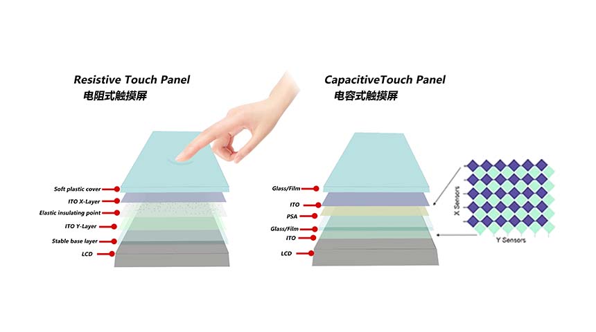
Capacitive and resistive touch screens present distinct electromagnetic interference challenges due to their underlying operating principles. Capacitive touch, being an active sensing technology, typically involves higher-frequency signals and more complex circuitry, making it more susceptible to both emitting and receiving interference. Resistive touch, a passive pressure-based technology, generally has a simpler, lower-frequency signal path, often resulting in a less complex EMC profile, though it is not immune to issues.
The capacitive touch screen functions by constantly measuring the capacitance of a grid of electrodes, a process driven by a microcontroller emitting periodic scanning signals often in the hundreds of kilohertz range. This active scanning can become a source of broadband noise if not properly filtered and shielded. Furthermore, the high-impedance sensor is exceptionally vulnerable to noise injection from external sources, which can manifest as ghost touches or reduced accuracy. In contrast, a resistive touch screen is a simple voltage divider activated only upon physical pressure; its DC-biased analog signal is inherently lower in frequency and less prone to radiating energy. However, the long, thin traces connecting the resistive film to the controller can act as efficient antennas for both emission and reception if not routed carefully. For instance, integrating a capacitive touch panel into a medical device requires meticulous attention to shielding to prevent its noise from disrupting sensitive bio-sensors in the same enclosure. Does the perceived simplicity of resistive technology lead to complacency in its EMC design? Can the advanced features of capacitive touch be realized without compromising the electromagnetic budget of the entire system? Therefore, the choice of technology directly influences the EMC mitigation tactics. A capacitive design may demand a continuous ground plane behind the sensor and ferrite beads on power lines, while a resistive design’s priority might be minimizing loop areas in the sensor trace routing.
What are the key pre-compliance testing steps for a touch module before formal lab submission?
Pre-compliance testing is a critical, cost-saving phase where developers identify and mitigate major EMC issues in-house before the expensive formal certification lab. Key steps include performing radiated and conducted emissions scans in a low-noise environment using a spectrum analyzer, verifying power integrity, and conducting basic immunity checks like electrostatic discharge simulation to uncover design vulnerabilities early in the development cycle.
Establishing a basic pre-compliance setup doesn’t require a million-dollar chamber; a quiet room, a spectrum analyzer with a near-field probe kit, and a line impedance stabilization network for conducted emissions can provide immense insight. The process begins with characterizing the power supply noise, as switching regulators are frequent culprits for conducted emissions failures. Using a near-field probe, you can then scan the surface of the touch display assembly and its flexible printed circuit connections to locate “hot spots” of electromagnetic radiation, often tracing back to clock signals or high-speed data lines to the display driver. A practical example is discovering that emissions spike at the refresh rate of the LCD panel, indicating a need for better filtering on the panel’s power input or shielding of its ribbon cable. What unseen noise is your prototype radiating that could doom a formal test? How can you correlate near-field probe readings with the far-field measurements required for official reports? Subsequently, after identifying issues, you implement fixes like adding shielding cans, strategically placing decoupling capacitors, or applying copper tape to cables, and then re-test to verify improvement. This iterative debugging loop is invaluable. It transforms the formal compliance test from a gamble into a confirmation of a well-engineered product, saving weeks of delay and thousands of dollars in lab re-test fees.
Which specific design strategies effectively reduce radiated emissions from a touch display assembly?
Effective strategies to curb radiated emissions focus on containing high-frequency energy at its source. This includes implementing a solid, low-impedance ground plane, using shielded flex cables or embedding critical signals between ground layers, applying ferrite beads and common-mode chokes on cables, ensuring proper decoupling for all integrated circuits, and employing conductive gaskets or coatings to create a continuous Faraday cage around the display module.
The fundamental principle is controlling the path of return currents. High-frequency currents follow the path of least inductance, not least resistance, which is often directly under the signal trace on an adjacent ground plane. A fractured or poorly connected ground forces these currents to take longer, loopier paths, effectively turning the printed circuit board traces into efficient radiating antennas. For a touch display, special attention must be paid to the interface between the touch controller board and the sensor itself. An unshielded flex cable can be a primary emission source; opting for a cable with built-in shielding layers, grounded at both ends, is a highly effective countermeasure. Furthermore, the LCD’s own driver circuitry and backlight inverter, especially in older CCFL designs, are notorious emitters. Selecting a display module with an integrated metal frame that makes solid contact with your product’s chassis can act as a built-in shield. Consider the analogy of a garden hose: if you kink the hose (add a ferrite choke), you restrict the flow of water (high-frequency noise) from reaching the sprinkler (the cable acting as an antenna). Have you accounted for the return current path for every signal on your display interface? Is your shielding strategy creating a complete enclosure or merely decorative pieces? Thus, a holistic approach that considers the entire current loop, from the driver IC, through the connector, across the cable, to the sensor and back, is essential. Partnering with a display provider like CDTech, which understands these constraints and can supply pre-tested modules with EMC-friendly designs, can significantly de-risk the process.
What role do component selection and supplier collaboration play in achieving EMC compliance?
Component selection and supplier collaboration are foundational to EMC success, as they determine the inherent noise characteristics of the system. Choosing displays with bonded optical filters that include transparent conductive coating for shielding, touch controllers with built-in spread spectrum features, and pre-certified wireless modules reduces the noise burden. Proactive collaboration with suppliers like CDTech to access technical design support and EMC test data for their modules is invaluable for streamlining certification.
| Component Category | EMC-Critical Feature to Specify | Impact on Compliance | Example Specification / Ask from Supplier |
|---|---|---|---|
| Display Module (LCD) | Integrated Shielding | Reduces radiated emissions from row/column drivers and backlight circuits; improves immunity. | Request module with a metal bezel or frame that provides a low-impedance grounding point, and ask for S-Parameter data for the LVDS interface. |
| Capacitive Touch Controller IC | Spread Spectrum Clocking (SSC) | Dithers the clock frequency to spread emitted energy over a wider band, lowering peak emissions below limits. | Select a controller with user-adjustable SSC modulation profiles to balance emission reduction with touch performance. |
| Power Management (LDO/Switcher) | Low-Noise Design & Filtering | Minimizes conducted noise on power rails, a common failure point; clean power is essential for sensitive touch sensing. | Choose regulators with high PSRR, and require the display module to include sufficient input filtering (e.g., pi-filters). |
| Flexible Printed Circuit (FPC) | Shielded Construction | Prevents the FPC from acting as an antenna for signals traveling between the main board and the touch sensor. | Specify an FPC with a laminated copper shield layer, with clear instructions on grounding points at both connectors. |
How does the integration environment (metal vs. plastic enclosure) affect the EMC testing approach?
The host device’s enclosure material drastically alters EMC strategy. A conductive metal enclosure naturally provides shielding, allowing designers to focus on sealing gaps and filtering cables that penetrate the shield. A non-conductive plastic enclosure offers no inherent shielding, forcing all emission control and immunity to be achieved at the board and module level, often requiring conductive coatings or internal metalized layers.
| Integration Factor | Metal Enclosure Strategy | Plastic Enclosure Strategy | Common Challenge & Mitigation |
|---|---|---|---|
| Shielding Principle | Exploit the enclosure as a Faraday cage. Ensure electrical continuity between panels. | Create shielding at the sub-assembly level. Use shielded modules or internal conductive paint/foil. | Grounding Strategy: Metal requires a star ground point; plastic requires a dedicated ground plane on the PCB. |
| Cable & Aperture Management | Focus on filtering all cables exiting the enclosure (USB, power, etc.) using feedthrough capacitors or filtered connectors. | Cables are less critical for emissions but remain immunity paths. Use common-mode chokes and robust connector grounding. | Display Cutout: A large opening for the screen is a major aperture. Use a transparent conductive coating (ITO) on the cover lens or a conductive gasket. |
| EMC Testing Focus | Verifying shield integrity. Tests often fail due to “leaks” from poorly sealed seams or unfiltered cables. | Achieving low emissions from the PCB itself. The board must pass as if it were fully exposed. | Pre-compliance: For metal, scan for leaks; for plastic, near-field probe the PCB and display directly. |
| Role of Display Module | The module can be less shielded internally, as the metal enclosure provides overall containment. | The display module itself must be a low-emitter. A pre-shielded module from CDTech becomes a critical component. | Cost-Benefit: A more expensive, fully shielded display module may be essential for a plastic enclosure to avoid costly secondary shielding processes. |
Expert Views
Navigating CE and FCC compliance for touch-integrated products is less about magic and more about methodical discipline. The most common pitfall I see is treating EMC as a validation step at the end of design, rather than a core requirement from the initial architecture. Success hinges on three pillars: a clean, well-layered PCB with meticulous attention to return paths; treating every cable and connector as a potential antenna that needs filtering or shielding; and choosing your display and touch partner wisely. A supplier that provides modules with EMC data, design-for-compliance guidance, and consistent manufacturing quality isn’t just a vendor; they are an extension of your engineering team. This collaboration turns certification from a stressful hurdle into a predictable milestone.
Why Choose CDTech
CDTech brings over a decade of specialized experience in display and touch integration directly to your design process. Their value lies in a deep understanding of the pain points associated with EMC compliance for interactive displays. They approach module design with EMI suppression in mind, offering solutions like displays with integrated EMF shielding and robust connector interfaces. This expertise translates into tangible benefits for your project: reduced pre-compliance debugging time, higher confidence ahead of formal testing, and ultimately, a more reliable end product. Their engineering support can provide critical insights into layout and grounding specific to their modules, helping you avoid common integration mistakes that lead to emission failures.
How to Start
Begin by defining your product’s target markets and thus the exact compliance standards (FCC, CE, and others) you must meet. Next, conduct an EMC risk assessment in your initial block diagram phase, identifying potential noise sources like display drivers and touch controllers. Engage with your display and touch technology provider early; share your compliance goals and request their module’s EMC test reports or design guidelines. Incorporate key EMC components (filtered connectors, shielding provisions) into your first mechanical and electrical prototypes. Finally, budget for and execute iterative pre-compliance testing as early as possible, using the findings to refine your design before the critical design freeze. This proactive, phased approach systematically de-risks the path to certification.
FAQs
Does using a pre-certified touch display module guarantee my final product will pass FCC/CE tests?
No, it does not guarantee final product compliance. A pre-certified or EMC-optimized module significantly reduces the risk and emission burden, but the final system’s integration—your PCB layout, power supply, cabling, and enclosure—ultimately determines the test outcome. The module is a critical component, but system-level design is paramount.
What is the most frequent cause of EMC test failure for devices with touch screens?
The most common failure points are radiated emissions from high-speed digital signals on the display interface (like LVDS or MIPI) and noise from the switching power supply that powers the backlight and logic boards. These issues often stem from poor grounding, inadequate filtering on power inputs, or unshielded flex cables acting as antennas.
How early in the product development cycle should we consider EMC for our touch device?
EMC considerations must start at the very beginning, during the product architecture and component selection phase. Decisions made here, such as choice of enclosure material, display technology, and controller ICs, set the foundation for EMC performance. Retrofitting fixes after a prototype fails testing is exponentially more costly and time-consuming.
Can we perform meaningful EMC pre-compliance testing without an anechoic chamber?
Yes, meaningful pre-compliance is possible without a full chamber. A spectrum analyzer with near-field probes can identify emission hotspots on your PCB and cables. A simple, quiet outdoor area or a room away from major RF sources can be used for basic radiated scans. The goal is comparative analysis—finding and fixing the biggest problems before the official test.
Achieving CE and FCC compliance for touch modules is a conquerable challenge through proactive design and informed partnership. The key takeaways are to integrate EMC principles from the initial concept, not as an afterthought; to understand that the enclosure material dictates your shielding strategy; and to leverage the expertise of component suppliers who can provide EMC-optimized building blocks. Treat every cable and connector as a potential leak, and invest in early, iterative pre-compliance testing to find and fix issues when changes are still cheap. By adopting this systematic approach, you transform regulatory compliance from a daunting barrier into a seamless step in your product’s journey to a global market.
Post Search
Related Articles
-
Capacitive vs Resistive Touch Screen Car Stereo: Which Is Right for You?
-
TN LCD vs IPS LCD: How to Choose the Right Display for You
-
Capacitive Touch Panel or Resistive: Which Suits Your Needs?
-
Why Choose an IPS LCD Panel for Your Next Screen Purchase?
-
CDTECH to Showcase Cutting-Edge Display Solutions at SID 2025
-
Comparing Different Types of Displays in Cars: A Detailed Overview
-
White Spots on LCD Screen: Causes, Fixes & Industrial Solutions (2026 Guide)