
How Is the JD9168S Display Driver Chip Shaping 2026 LCD Display Design?
 2026-05-02
  21:23
21:23 

The JD9168S is an a‑Si TFT LCD driver IC supporting up to 800×480 WVGA resolution that enables compact, cost‑effective display modules for industrial, medical, and consumer devices. As the global DDIC market stabilizes in 2026, this driver gives designers a solid, low‑BOM solution for mainstream TFT‑LCD panels without moving to OLED‑class platforms. Companies such as CDTech build standardized LCD modules around JD9168S to offer reliable, long‑life display nodes for OEMs across multiple application segments.
What Is the JD9168S Display Driver Chip?
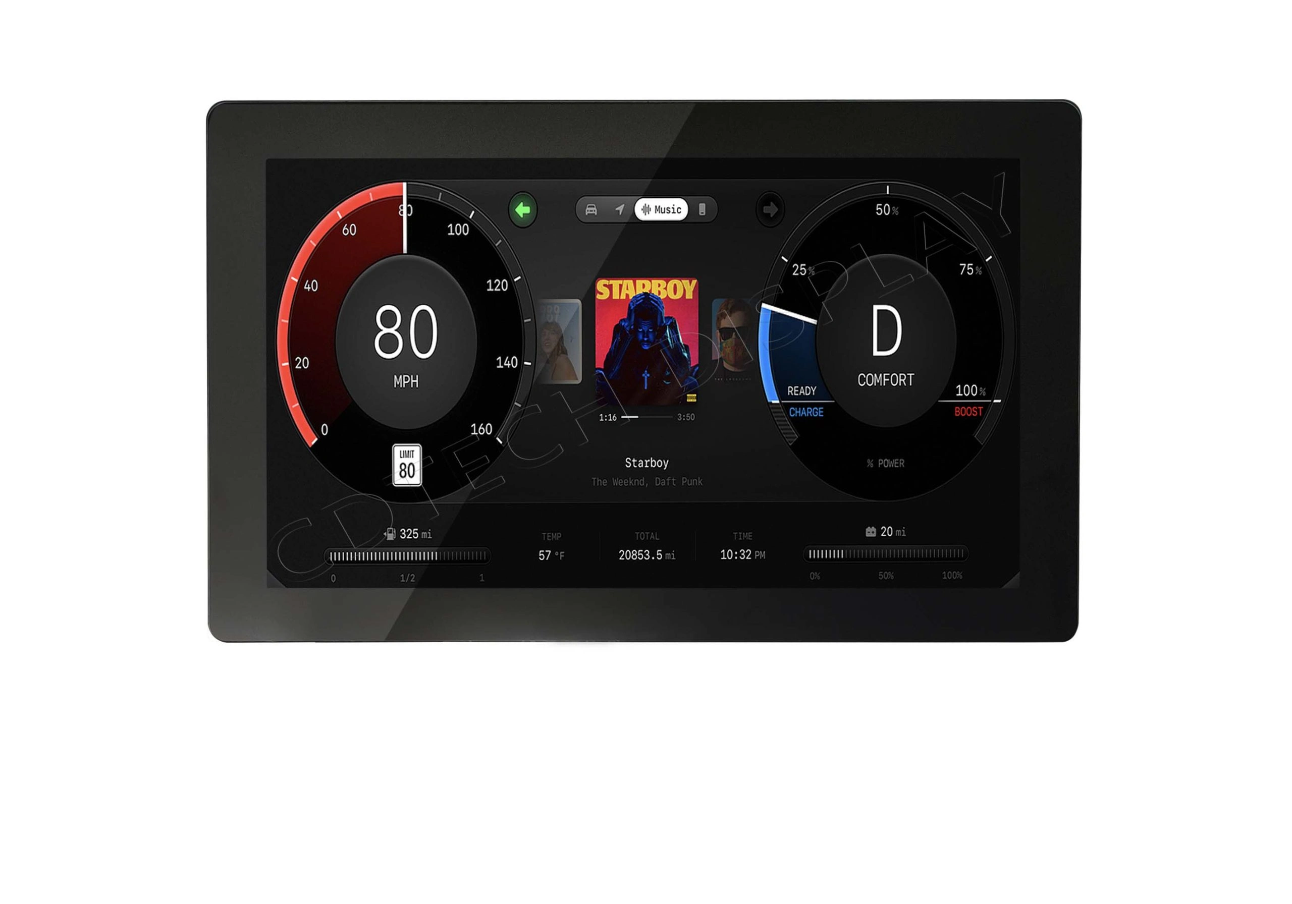
The JD9168S is a single‑chip display driver IC designed for a‑Si TFT LCDs, supporting up to 800×480 WVGA resolution with 16.7M‑color capability and no internal frame memory. It integrates on‑chip gamma control, several power‑generation modes, and multiple digital interfaces (RGB, LVDS, and MIPI DSI) so system designers can simplify module architecture and reduce external component count. This makes JD9168S suitable for compact, robust LCD modules used in operator panels, medical devices, and consumer electronics.
Because the chip is built specifically for a‑Si TFT, it pairs well with cost‑sensitive, mid‑size displays around 5–6 inches. Designers often choose JD9168S when they need a balance of image quality, wide‑temperature operation, and compatibility with mainstream LCD‑panel partners such as CDTech and other module manufacturers that supply drop‑in‑ready TFT‑LCD nodes.
Why Is the JD9168S Well‑Suited for a‑Si TFT LCD Applications?
JD9168S is optimized for a‑Si TFT LCDs by integrating the full driver pipeline—from command decoding and timing control to source and gate driving—into a single package. Its built‑in DC‑DC charge‑pump structures allow AVDD/AVEE (and sometimes VGH/VGL) generation from a single external supply, reducing the need for external power ICs and simplifying PCB layout. This compact power architecture suits standard‑resolution industrial and automotive displays where space and thermal management are critical.
The chip also supports wide‑temperature‑range operation and multiple interface modes such as SPI, I²C, RGB, LVDS, and DSI, which aligns well with the mixed‑signal environments typical of a‑Si‑based HMIs and control panels. Vendors such as CDTech design a‑Si TFT LCD modules around JD9168S to deliver standardized, plug‑and‑play display solutions that minimize NRE and firmware porting effort for OEMs.
How Do RGB, LVDS, and DSI Interfaces Affect JD9168S‑Based Designs?
JD9168S supports RGB, LVDS, and MIPI DSI interfaces, giving engineers multiple ways to route graphics data from host processors into the panel. RGB mode offers simple parallel timing that matches many microcontrollers and embedded CPUs, while LVDS improves signal integrity and noise immunity over longer traces, making it suitable for larger control panels and industrial cabinets. DSI mode enables low‑EMI, high‑speed serial links common in modern SoC‑based platforms, especially in IoT and handheld devices.
Each interface alters the design trade‑offs. RGB‑based modules are easier to validate and debug but require more CPU pins; LVDS versions reduce pin count and EMI at the cost of more complex layout rules; DSI‑only designs benefit from SerDes‑style wiring but require protocol‑aware firmware and timing tuning. Many CDTech‑engineered LCD modules expose multiple interface options so customers can choose the best fit for their carrier‑board ecosystem.
Typical Interface Modes on JD9168S‑Based LCD Modules
How Does JD9168S Support 16.7M Color and Gamma Control?
The JD9168S supports up to 16.7M colors by driving 18‑bit or 24‑bit RGB pixel formats over its RGB, LVDS, or DSI interfaces and mapping them to the panel’s sub‑pixel matrix. Its internal gamma‑adjustment structure lets designers tune grayscale linearity and color balance via a set of programmable registers, enabling consistent brightness and color reproduction across different panel lots and operating temperatures. This capability is important for human‑visible UIs where image fidelity matters.
For many manufacturers, including CDTech, the gamma‑register table simplifies display calibration because the module can be pre‑tuned at the factory while still allowing field‑ or application‑level tweaks. The absence of embedded frame memory means all frame data comes from the host, but the JD9168S’s command‑based brightness and display‑control functions give OEMs fine‑grained control over viewing experience without extra controller silicon.
How Does Market Stabilization in 2026 Benefit JD9168S‑Based Modules?
Global DDIC shipments are projected to stabilize in 2026 after a slight dip in 2025, with particular recovery in LCD TV panels driven by 4K+ resolutions and dual‑/triple‑rate driving technologies. While OLED‑centric markets grow, the continued dominance of TFT‑LCD in industrial, automotive HMI, and consumer‑electronic “standard‑resolution” segments creates sustained demand for cost‑efficient a‑Si drivers such as JD9168S.
For module suppliers, this means renewed investment in LCD‑based value‑engineered platforms instead of aggressive OLED‑only upgrades. Companies like CDTech can leverage JD9168S to offer standardized, high‑volume LCD modules with proven reliability and wide‑temperature performance, aligning with the 2026 preference for stable, cost‑effective display solutions over premium‑only technologies.
How Are Cost‑Effective LCD Solutions Shaping 2026 Designs?
As smartphone and notebook markets absorb high‑end OLED drivers, LCD panels and supporting DDICs are becoming more attractive for non‑premium segments where reliability, supply‑chain resilience, and unit cost dominate. The JD9168S fits this trend by supporting 640×480 and 800×480 resolutions at a per‑chip cost that is lower than high‑frame‑rate OLED‑targeted drivers, while still enabling 16.7M‑color output and robust on‑board power management.
Designers increasingly pair JD9168S with RGB‑888 or 18‑bit LVDS interfaces to deliver decent‑quality GUIs on 5–6 inch panels in industrial HMIs, medical devices, and vending/machine‑control panels. Chinese and global OEMs also favor this architecture because it allows faster design‑to‑volume cycles and easier substitution of hosts or microcontrollers without redoing the LCD‑side driver stack.
How Does JD9168S Work With Capacitive Touch Panels?
Many LCD modules built around JD9168S integrate separate capacitive‑touch‑panel (CTP) controllers such as GT911, which communicate with the host MCU via I²C, while the JD9168S remains focused on driving the TFT. This clear separation avoids coupling touch‑related firmware logic into the driver IC and lets designers reuse existing I²C touch‑stacks across multiple display platforms.
CDTech and similar vendors often package JD9168S‑based LCDs with 5‑point CTPs, yielding slim multi‑touch enablement for handheld devices and operator panels. The standalone‑driver approach keeps the module architecture modular: if the end‑user decides to upgrade to a different touch controller or sensor, the core LCD driver side remains unchanged, reducing risk and requalification effort.
How Can Engineers Optimize Layout and Power When Using JD9168S?
JD9168S data materials define maximum layout resistances and recommend controlled‑impedance routing for LVDS and DSI lanes, plus careful power‑plane and decoupling strategies for AVDD/AVEE and VGH/VGL rails. Layouts that respect these constraints exhibit fewer noise‑related artifacts and better EMI performance, especially in mixed‑signal environments such as industrial controllers and medical equipment.
For power, designers can choose between internal‑charge‑pump‑only modes and external‑supply‑plus‑charge‑pump modes depending on efficiency requirements and thermal constraints. External‑power topologies with external DC‑DC converters can reduce on‑chip dissipation and improve thermal headroom, a strategy that many CDTech‑designed modules adopt for wide‑temperature‑range applications.
How Does JD9168S Fit Into 2026 Lifecycle and Maintenance Planning?
As a dedicated a‑Si TFT driver with multiple interface options and a stable feature set, JD9168S supports long‑life product families spanning 5–10 years in industrial automation, medical devices, and embedded control systems. The absence of integrated frame memory keeps the chip architecture simpler and less likely to require rapid obsolescence‑driven redesigns compared to highly integrated display‑controller‑SoCs.
Module makers such as CDTech help customers manage lifecycle risk by offering standardized JD9168S‑based LCD form factors, documented interface timing, and service‑oriented support for panel revisions and brightness‑/color‑related re‑tuning. This makes JD9168S a practical choice for teams that want to lock in a display platform early and extend it across multiple product generations.
What Are Practical Design Tips for Using JD9168S in New Products?
When incorporating JD9168S into new designs, start with a reference timing diagram for RGB or DSI and verify the host‑side pixel clock and sync timing against the chip’s specific tables to avoid tearing and flicker. Use the chip’s built‑in self‑diagnostic registers for power‑on tests to validate panel and driver hand‑shake cleanly. Keep LVDS and DSI traces as short as possible and matched in length, and apply the recommended termination and impedance rules to avoid data‑rate limitations.
For designs oriented toward wide‑temperature or industrial conditions, select a CDTech‑style module that already incorporates robust backlight‑driver and thermal‑design practices, then focus firmware on brightness, gamma, and touch‑controller integration. This approach accelerates time‑to‑market while preserving flexibility for later UI‑layer updates.
CDTech Expert Views
“CDTech views the JD9168S as a strategic a‑Si TFT driver for our mid‑range LCD module portfolio because it supports mainstream resolutions, 16.7M‑color output, and flexible power‑system options while keeping the BOM manageable. As the 2026 DDIC market stabilizes, we are seeing renewed demand for cost‑effective LCD panels paired with reliable, single‑chip drivers that can run across multiple host platforms and industrial‑grade environments. By combining JD9168S with our 2nd‑cutting‑technology‑enabled bezel designs and integrated CTP stacks, CDTech delivers application‑ready modules that reduce our customers’ development time and supply‑chain risk without sacrificing display quality.”
How JD9168S Fits into 2026 LCD Display Strategy
The JD9168S represents a sweet spot in the 2026 display‑driver landscape: a mature, cost‑effective a‑Si TFT driver that supports WVGA‑class resolutions and multiple interface standards while feeding into the broader trend of LCD‑based value‑engineering. As the global DDIC market stabilizes and certain LCD‑segment demand rebounds, chips like JD9168S help OEMs avoid over‑spec’ing their displays with OLED‑only solutions and instead deploy robust, long‑life LCD modules for industrial, medical, and consumer‑control applications.
Manufacturers such as CDTech leverage this balance by offering standardized 5–6 inch LCD modules with JD9168S, RGB‑888, LVDS, or DSI interfaces, and integrated CTP layers, enabling OEMs to focus on software and product differentiation. For 2026‑era projects, selecting JD9168S‑based platforms means investing in a proven, service‑oriented ecosystem that supports lifecycle planning, thermal and EMI robustness, and long‑term supply security.
Frequently Asked Questions
How resolution flexible is the JD9168S?
The JD9168S supports up to 800×480 WVGA‑class resolutions (with a maximum capability of 1024×1024 per its data sheet), making it suitable for 5–6 inch standard‑resolution TFT LCDs used in HMIs and embedded devices. Many LCD‑module vendors, including CDTech‑style partners, tune the chip for 640×480 or 800×480 panels to balance pixel density and processor‑load requirements.
Does JD9168S include internal frame memory?
No; the JD9168S is a driver‑only IC without internal frame memory, meaning all frame data must be pushed continuously from the host processor via RGB, LVDS, or MIPI DSI. This design reduces chip complexity and keeps the memory hierarchy in the host system, which simplifies firmware reuse across multiple display platforms.
What is the role of gamma control in JD9168S?
The JD9168S provides programmable gamma‑adjustment registers that allow fine‑tuning of grayscale levels and color balance, improving image uniformity and reducing panel‑to‑panel variability. Designers and module makers such as CDTech normally calibrate these registers during module bring‑up, enabling consistent brightness and color performance across different panel batches and temperature ranges.
Can JD9168S be used in wide‑temperature‑range applications?
Yes; many LCD modules using JD9168S are specified for operating ranges around –30°C to +80°C, making them suitable for industrial and outdoor‑facing applications. The chip’s internal power‑generation and self‑diagnostic features help maintain stable panel operation across these extremes, especially when combined with robust backlight‑driver and thermal‑design practices from vendors like CDTech.
How easy is it to migrate from other WVGA drivers to JD9168S?
Migration is relatively straightforward when the new board supports the same interface (RGB, LVDS, or DSI) and meets the required timing constraints. Because JD9168S exposes a standard‑command‑set‑style interface for display control and brightness, designers can often reuse much of their existing LCD‑driver firmware, then adapt only the timing and gamma‑tuning layers for the new panel. This makes JD9168S a practical drop‑in alternative within the broader a‑Si TFT driver ecosystem.
Post Search
Related Articles
-

Capacitive vs Resistive Touch Screen Car Stereo: Which Is Right for You?
-
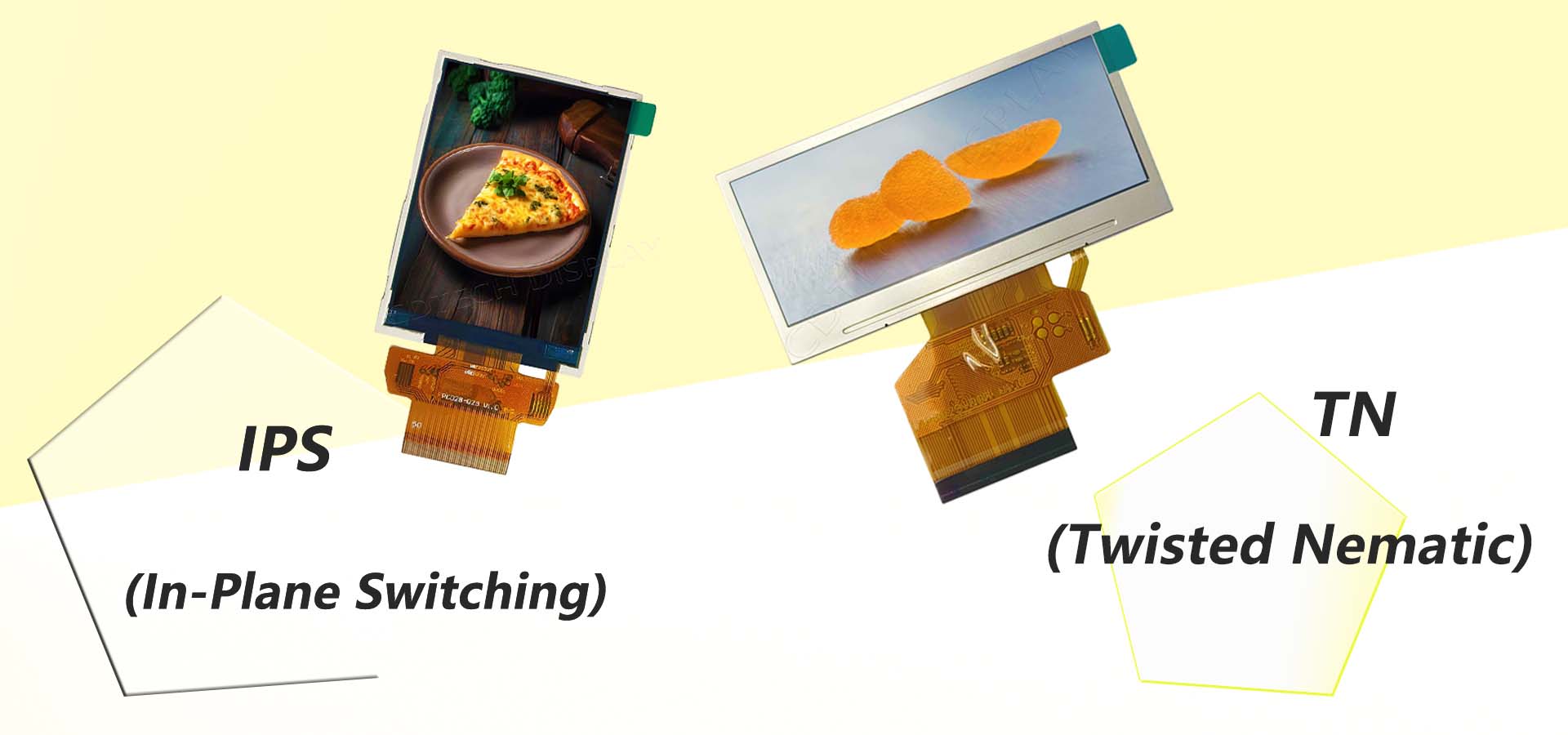
TN LCD vs IPS LCD: How to Choose the Right Display for You
-
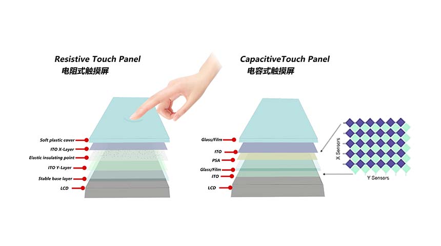
Capacitive Touch Panel or Resistive: Which Suits Your Needs?
-
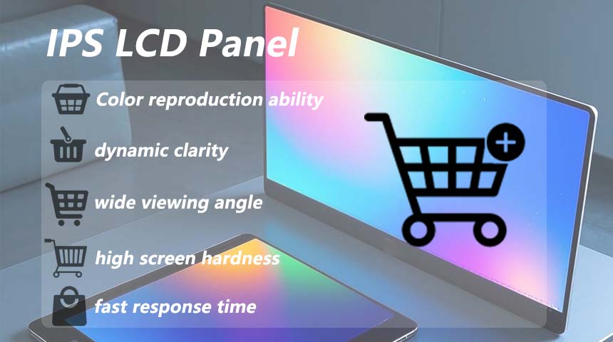
Why Choose an IPS LCD Panel for Your Next Screen Purchase?
-
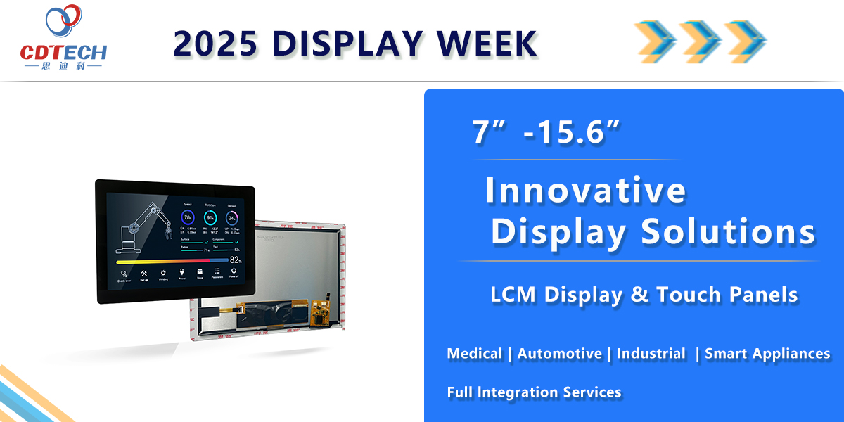
CDTECH to Showcase Cutting-Edge Display Solutions at SID 2025
-
Comparing Different Types of Displays in Cars: A Detailed Overview
-
White Spots on LCD Screen: Causes, Fixes & Industrial Solutions (2026 Guide)