Why Are Touch ICs Moving to 40nm HV CMOS in 2026?
 2026-04-29
  20:55
20:55 

As of Q2 2026, leading touch IC makers, including Ilitek, have shifted high‑performance capacitive touch controllers from legacy nodes to advanced 40nm High‑Voltage (HV) CMOS processes. This supply‑chain optimization relieves wafer‑capacity pressure, improves power efficiency by 15–20%, and sustains the high driving voltages needed for large industrial panels.
ILI2132 Single Chip Capacitive Touch Panel Controller Data Sheet
How has 40nm HV CMOS improved touch‑IC power efficiency?
Transitioning to 40nm HV CMOS lowers active and leakage power in sensor read‑out channels, charge‑pump stages, and digital logic blocks, delivering 15–20% better energy efficiency versus older 65nm or 90nm nodes. The finer geometry and advanced gate‑stack materials reduce gate capacitance and leakage, so controllers such as the ILI2132 can drive high‑voltage signals without a proportional rise in current draw.
From a system viewpoint, industrial HMI stacks benefit from lower operating and standby power, which reduces heat buildup in sealed enclosures and improves long‑term reliability. This power‑efficiency leap is especially valuable for CDTech‑designed rugged displays deployed in automation cabinets, medical equipment, and outdoor kiosks where thermal management is critical.
What does “HV CMOS process” mean for touch ICs?
An HV CMOS process is a standard CMOS flow enhanced to support high‑voltage devices (typically 10–20 V) while retaining low‑voltage logic and I/O on the same die. For touch controllers like the ILI2132, this enables integration of high‑voltage transistors for the on‑chip 10 V AVDD_CP charge pump alongside 1.8–3.3 V logic without sacrificing yield or reliability.
From a design standpoint, HV CMOS removes the need for external high‑voltage buffers and level‑shifters around the controller, simplifying the surrounding circuit. That reduction in passive and driver components improves board‑level reliability and EMI performance, which is one of the reasons CDTech prefers 40nm HV CMOS‑based touch solutions for industrial HMI assemblies.
Why are manufacturers shifting to 40nm from legacy nodes?
Legacy nodes such as 90nm and older 65nm are facing tight wafer‑capacity constraints, as foundries prioritize higher‑margin logic, RF, and automotive wafers. The 40nm node, in contrast, offers a stable, high‑yield flow on 300 mm wafers, which supports higher throughput and better economics for high‑volume touch‑IC production.
By migrating to 40nm, companies like Ilitek secure longer‑term allocations and more predictable pricing for touch controllers, which directly benefits industrial HMI module suppliers such as CDTech. This substrate stability also eases the redesign of legacy systems onto 40nm‑based controllers without changing the overall HMI interface or panel architecture.
Main drivers of the legacy‑to‑40nm move
-
Shrinking availability of 90nm and older 65nm wafer capacity
-
Mature 40nm processes with proven defect‑density and yield profiles
-
Lower cost per die than smaller‑geometry advanced nodes
How do wafer capacity and 40nm lines affect industrial HMIs?
Expanded 40nm HV CMOS wafer capacity translates into more predictable lead times and higher volume availability for touch controllers, which is essential for long‑running industrial HMI programs. With less competition for 90nm slots, manufacturers can secure multi‑year agreements for parts such as the ILI2132, ensuring stable BOMs for production lines.
For OEMs, this means fewer design‑re‑spins, more consistent pricing, and easier integration of new touch‑panel stacks. CDTech leverages this stable 40nm environment to offer pre‑characterized TFT‑CTP modules that pair 40nm‑based controllers with rugged LCDs, simplifying qualification and reducing time‑to‑market for industrial HMI projects.
What makes 40nm better for industrial‑panel driving performance?
Industrial‑size touch panels often require higher drive voltages and stronger sensing signals to overcome noise, thick overlays, and glove‑mode or stylus inputs. The 40nm HV CMOS node maintains robust high‑voltage drive capability while shrinking the digital logic footprint, allowing more sensing channels and advanced algorithms without increasing power or package size.
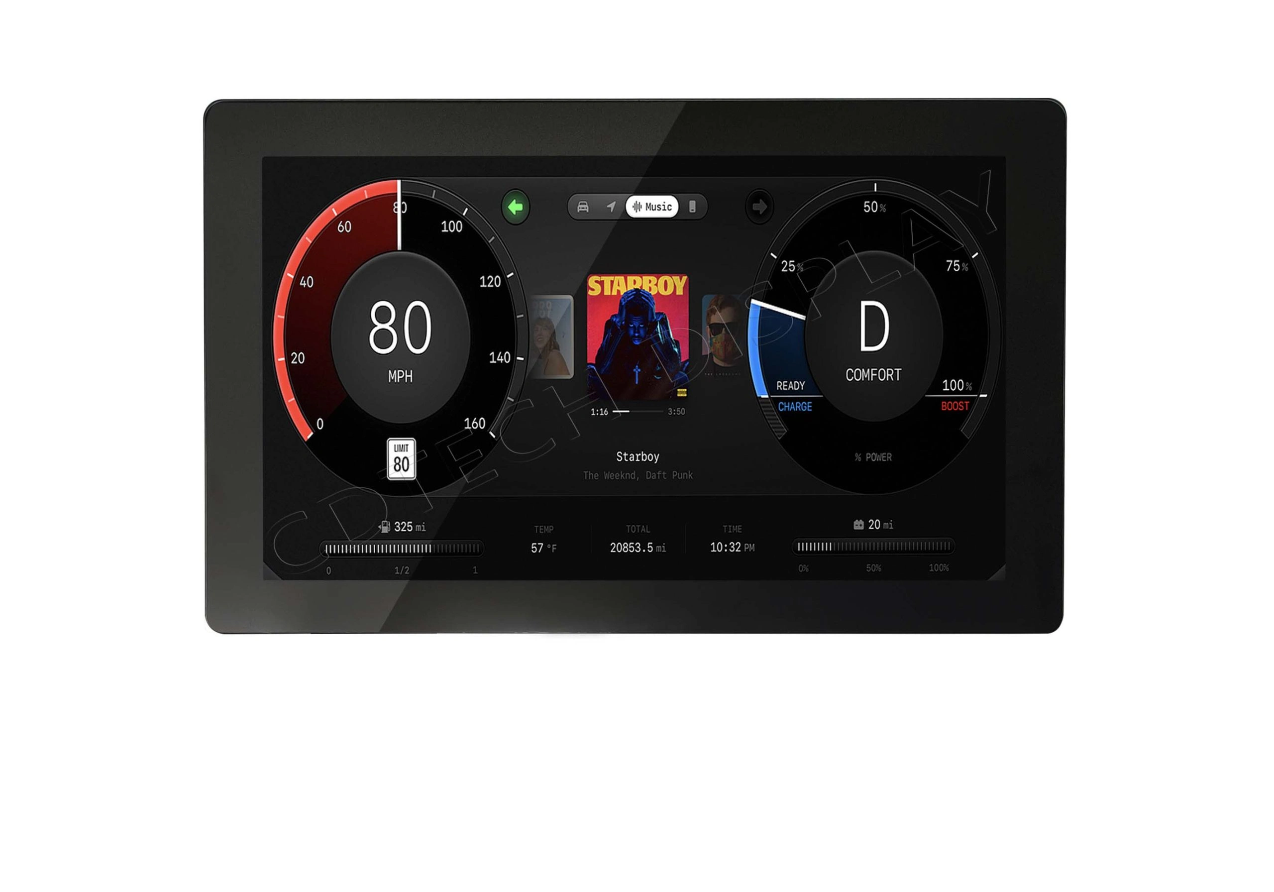
For example, the ILI2132 series can drive larger‑format industrial displays using its integrated x5 AVDD_CP charge pump, which delivers 10 V to the panel electrodes while keeping internal logic at low voltage. CDTech regularly pairs this controller with rugged‑grade TFTs and capacitive‑touch layers, creating HMI stacks that stay responsive in electrically noisy factory environments and under mechanical vibration.
Key performance advantages of 40nm for industrial panels
-
Higher number of sensing channels per package
-
Better immunity to EMI and environmental noise
-
Faster response for multi‑touch gestures and rapid touch events
How does the ILI2132 benefit from 40nm HV CMOS?
The ILI2132 is a high‑performance capacitive touch controller with 57 sensing channels, USB, I2C, and SPI interfaces, and integrated flash, packaged in a compact BGA‑90. Moving its production to 40nm HV CMOS improves its power efficiency, reduces internal voltage droop under heavy illumination or high‑noise conditions, and stabilizes the x5 AVDD_CP charge pump that supplies 10 V to the sensing electrodes.
This process upgrade also enhances yield and reliability, making ILI2132‑based modules suitable for mission‑critical applications such as medical HMIs, transportation control panels, and process‑automation interfaces. CDTech‑designed display‑and‑touch solutions that adopt ILI2132‑based stacks benefit from higher performance margins and lower long‑term replacement risk, supported by the mature 40nm supply chain.
ILI2132‑specific gains from 40nm migration
-
More stable 10 V AVDD_CP output under varying load
-
Lower internal noise coupling between charge‑pump and sensor logic
-
Easier long‑term sourcing for multi‑year product lifecycles
Why is 40nm stabilization good news for ILI2132 users?
With 40nm HV CMOS now stabilized across major foundries, ILI2132 users gain access to a more predictable supply chain, extended part availability, and potentially lower unit costs over time. Industrial HMI designers can plan multi‑year product roadmaps knowing that the controller’s process node is not at risk of rapid obsolescence.
For panel‑module integrators such as CDTech, this stability simplifies supply‑chain planning and the qualification of replacement or upgrade paths. CDTech often pre‑validates 40nm‑based ILI2132‑compatible touch stacks so customers can quickly migrate legacy controllers into new designs without re‑qualifying the entire LCD‑touch subsystem. This approach reduces redesign risk and accelerates time‑to‑market for industrial HMI upgrades.
How can engineers design for long‑term 40nm touch‑IC availability?
To maximize the benefit of 40nm stabilization, engineers should standardize on a single 40nm‑supplied HV touch controller platform, such as the ILI2132 series, across multiple product families and work with module‑level partners that decouple the controller from the LCD‑touch stack. Standardized interfaces reduce the number of unique BOMs and simplify lifecycle transitions when suppliers refresh or phase‑out discrete parts.
CDTech supports this strategy by offering mechanically and electrically modular 40nm‑based modules, allowing customers to reuse the same LCD‑touch form factor while updating only the controller firmware or software. This design‑for‑supply‑chain approach helps industrial HMI OEMs extend product lifetimes without sacrificing performance or reliability.
What are the cost‑effectiveness implications of 40nm HV CMOS?
Although 40nm process tools are more capital‑intensive than older 90nm lines, 300 mm wafers, higher die density, and strong yields reduce the effective cost per touch‑IC die over time. In industrial HMI programs with moderate to high volumes, these savings translate into lower BOM costs and more predictable pricing.
For CDTech‑designed display solutions, adopting 40nm‑based controllers such as the ILI2132 family allows the company to offer competitive pricing on rugged TFT‑CTP modules without compromising quality. Customers gain access to high‑performance, long‑life HMI platforms that balance upfront cost with reliability, certification overhead, and long‑term serviceability.
How does CDTech leverage 40nm HV CMOS in its solutions?
CDTech integrates 40nm HV CMOS‑based touch controllers, including ILI2132‑family variants, into its custom TFT LCD and capacitive‑touch assemblies to deliver robust, power‑efficient industrial HMIs. By combining advanced 40nm controllers with its proprietary 2nd‑cutting LCD technology, CDTech can offer unique form factors and resolutions tailored to specialized automation, medical, and outdoor applications.
CDTech also maintains close collaboration with foundry‑ and OSAT‑level partners that support 40nm HV CMOS, enabling long‑term supply agreements and migration paths for customers. This ecosystem‑aware strategy helps OEMs consolidate their display‑and‑touch supply chains with a single qualified partner, reducing component complexity and qualification overhead for industrial HMI projects.
CDTech Expert Views
“From CDTech’s perspective, the shift to 40nm HV CMOS represents a rare win–win moment: industrial‑HMI designers gain both higher performance and better supply‑chain predictability,” says a CDTech senior display‑and‑touch engineer. “By standardizing on 40nm‑based controllers such as Ilitek’s ILI2132 series, we can offer customers modular, power‑efficient touch stacks that are easier to qualify, maintain, and upgrade over a ten‑year product lifecycle without redesigning the entire machine interface.”
How can customers future‑proof their HMI designs now?
Customers can future‑proof their HMIs by choosing a 40nm HV CMOS‑based touch controller platform, partnering with a single display‑and‑touch integrator such as CDTech, and establishing a clear obsolescence‑management strategy from the outset. This includes defining standard mechanical and electrical interfaces, documenting second‑sourcing options, and planning for firmware‑level upgrades rather than frequent hardware changes.
Such a strategy ensures that new industrial HMI projects launched in 2026 will remain viable into the 2030s, even as wafer‑capacity balances shift again. CDTech’s engineering teams routinely help customers design these migration paths, making it easier to adopt 40nm‑based ILI2132‑style solutions without sacrificing time‑to‑market.
Key takeaways and actionable advice
-
Standardize on 40nm HV CMOS touch controllers such as ILI2132 for new industrial HMI designs to gain better power efficiency and long‑term supply stability.
-
Work with a display‑and‑touch integrator like CDTech that offers pre‑validated 40nm‑based TFT‑CTP modules to reduce redesign and qualification effort.
-
Define clear obsolescence and upgrade policies early, focusing on interface standardization and modular, firmware‑upgradable designs.
-
Monitor 40nm capacity trends and secure long‑term agreements where possible to protect multi‑year product programs.
Frequently Asked Questions
Q: What is the main benefit of moving touch ICs to 40nm HV CMOS?
A: The main benefit is 15–20% better power efficiency and more stable high‑voltage driving for industrial panels, while reducing risk from wafer‑capacity shortages at legacy nodes.
Q: Why is ILI2132 well suited for industrial HMIs?
A: ILI2132 combines a 10 V AVDD_CP charge pump, 57 sensing channels, and multiple interfaces in a compact package, making it ideal for large, noise‑prone industrial panels. Its migration to 40nm HV CMOS improves efficiency and long‑term supply stability.
Q: How does 40nm affect my HMI BOM cost?
A: Although 40nm tooling is more expensive, 300 mm wafers and higher die density typically lower the per‑die cost over time, especially in high‑volume industrial‑HMI programs supported by partners such as CDTech.
Q: Can CDTech help me migrate from older touch controllers to 40nm?
A: Yes; CDTech offers pre‑validated 40nm‑based TFT‑CTP modules and can assist with schematic, layout, and firmware migration, helping customers switch from legacy 65nm or 90nm controllers to 40nm HV CMOS platforms like ILI2132 with minimal redesign.
Q: Will 40nm touch controllers still be available in five years?
A: Yes; 40nm HV CMOS is expected to remain a mainstream node for industrial‑grade ICs through at least the early 2030s, supported by ongoing 300 mm wafer‑capacity investments and stable yields.
Post Search
Related Articles
-
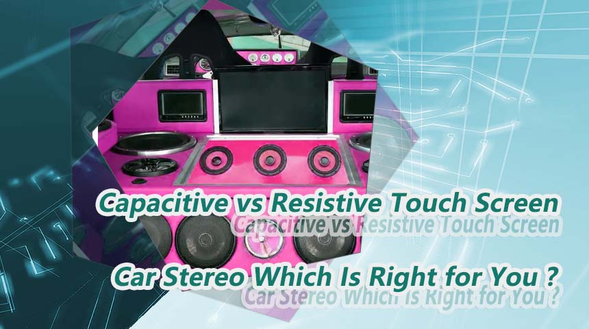
Capacitive vs Resistive Touch Screen Car Stereo: Which Is Right for You?
-
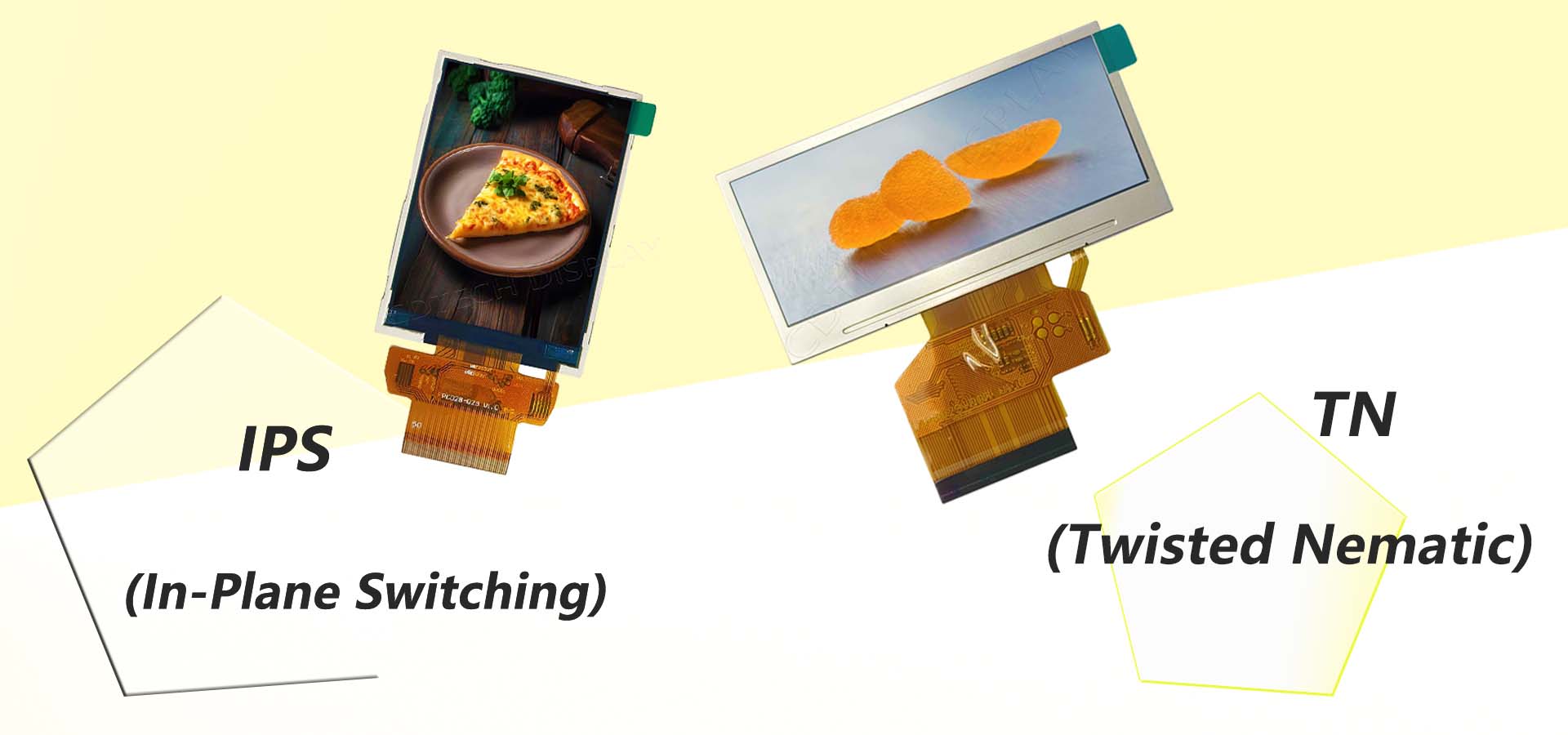
TN LCD vs IPS LCD: How to Choose the Right Display for You
-
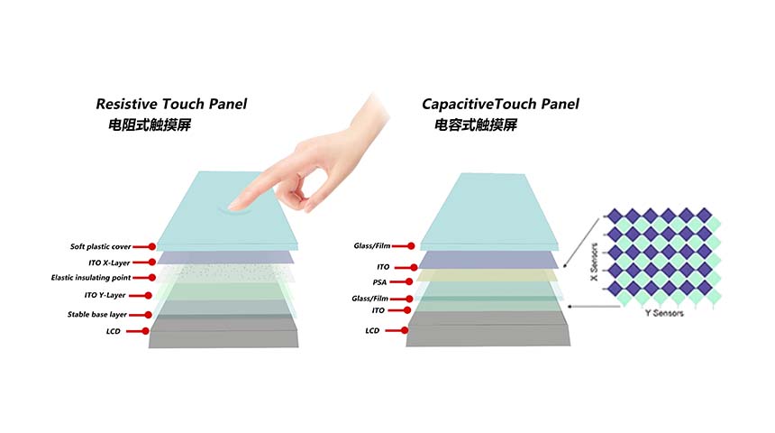
Capacitive Touch Panel or Resistive: Which Suits Your Needs?
-
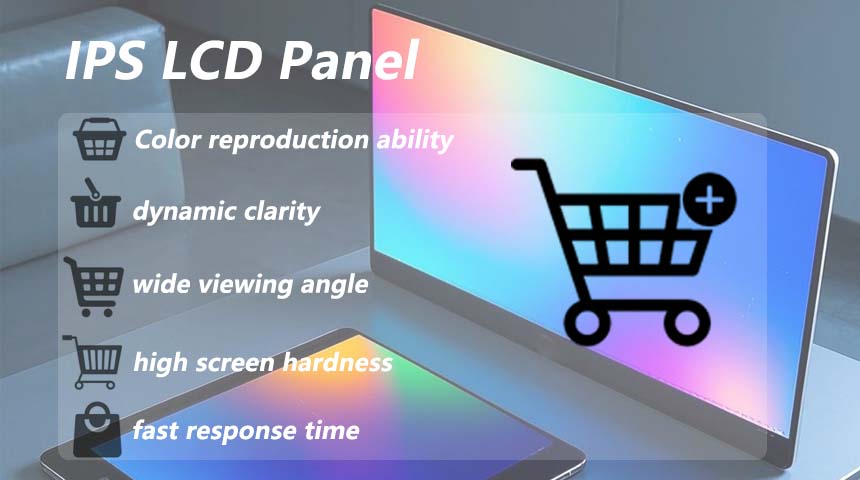
Why Choose an IPS LCD Panel for Your Next Screen Purchase?
-
CDTECH to Showcase Cutting-Edge Display Solutions at SID 2025
-
Comparing Different Types of Displays in Cars: A Detailed Overview
-
White Spots on LCD Screen: Causes, Fixes & Industrial Solutions (2026 Guide)