How Do Smart Surfaces Transform Automotive Cockpits in 2026?
 2026-06-06
  12:24
12:24 

Smart surfaces integrate LCD or MiniLED displays beneath woodgrain, fabric, or textured materials to illuminate icons seamlessly. At CES 2026, manufacturers like BOE and Tianma demonstrated this trend, but embedding screens into rigid decorative materials creates mechanical stress that causes white spots. Precision optical bonding and custom LCD sizing through 2nd Cutting technology prevent pressure-induced defects in automotive cockpits.
What Are Smart Surfaces and Why Are They Emerging at CES 2026?
Smart surfaces are decorative interior panels that hide embedded displays beneath fabric, wood, leather, or textured plastic, illuminating icons only when activated. At CES 2026, this automotive cockpit trend exploded as OEMs sought premium aesthetics without visible screen bezels, with BOE showing microLED versions and Tianma using QD miniLED LCDs in woodgrain surfaces.
The technology solves a critical design paradox: drivers want luxurious, traditional materials but need modern digital interfaces. Traditional cockpits featured exposed LCDs with visible borders, but smart surfaces conceal displays completely until backlit. This requires embedding TFT LCD panels directly beneath rigid decorative layers, creating unique engineering challenges for suppliers.
CDTech’s Shenzhen facility has addressed similar integration hurdles for automotive clients since 2011. In one anonymized case, a custom 7.2-inch automotive TFT cluster required non-standard dimensions that off-the-shelf 7.0″ panels couldn’t satisfy. Using patented 2nd Cutting technology, CDTech achieved a 17% yield improvement by precision-cutting the unique aspect ratio from mother glass, eliminating the mechanical stress that would have caused white spots in a standard panel forced into an improper enclosure.
The smart surface market distinguishes itself through material integration. Unlike conventional displays, these panels must maintain optical clarity through multiple material layers while resisting mechanical pressure from the rigid decorative overlay. This demands advanced optical bonding (OCA/LOCA) and precise enclosure tolerance control—exactly the engineering challenges CDTech solves for international OEM procurement teams sourcing from China.
How Does Mechanical Pressure Cause White Spots in Embedded Displays?
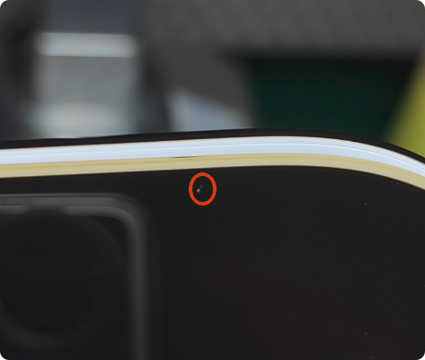
Mechanical pressure is the most common cause of white spots on LCD screens, resulting from tight enclosure designs, improper mounting, or structural stress between housing and screen. When decorative materials like wood or textured plastic press against the underlying LCD cell, localized pressure deforms internal layers, creating visible bright patches that worsen under temperature fluctuations.
White spots differ fundamentally from dead pixels. Dead pixels appear as fixed black or white dots from transistor failure, while white spots present as irregular bright areas that may change when pressed. This distinction matters for procurement: white spots indicate mechanical or optical design flaws requiring structural redesign, not simple panel replacement.
In automotive smart surface applications, the risk escalates because rigid decorative materials (woodgrain, carbon fiber, textured plastic) exert continuous pressure on the LCD. As 2026 vehicle cockpits shift toward embedding displays directly into these materials, controlling mechanical stress becomes the primary engineering challenge. CDTech’s CTP (Capacitive Touch Panel) integration process includes stress-testing protocols specifically for embedded applications, ensuring uniform mechanical support and avoiding localized stress concentration that causes white spots.
The manufacturing perspective reveals compounding factors: backlight module misalignment, contaminated diffuser films, inconsistent liquid crystal alignment from particles, and temperature fluctuations affecting layer stability. At CDTech’s 3,500m² Class 1,000 dust-free workshop in Shenzhen, Automated Optical Inspection (AOI) achieves <0.1% defect rates by detecting these issues before shipment.
Which TFT LCD Technologies Work Best for Automotive Smart Surfaces?
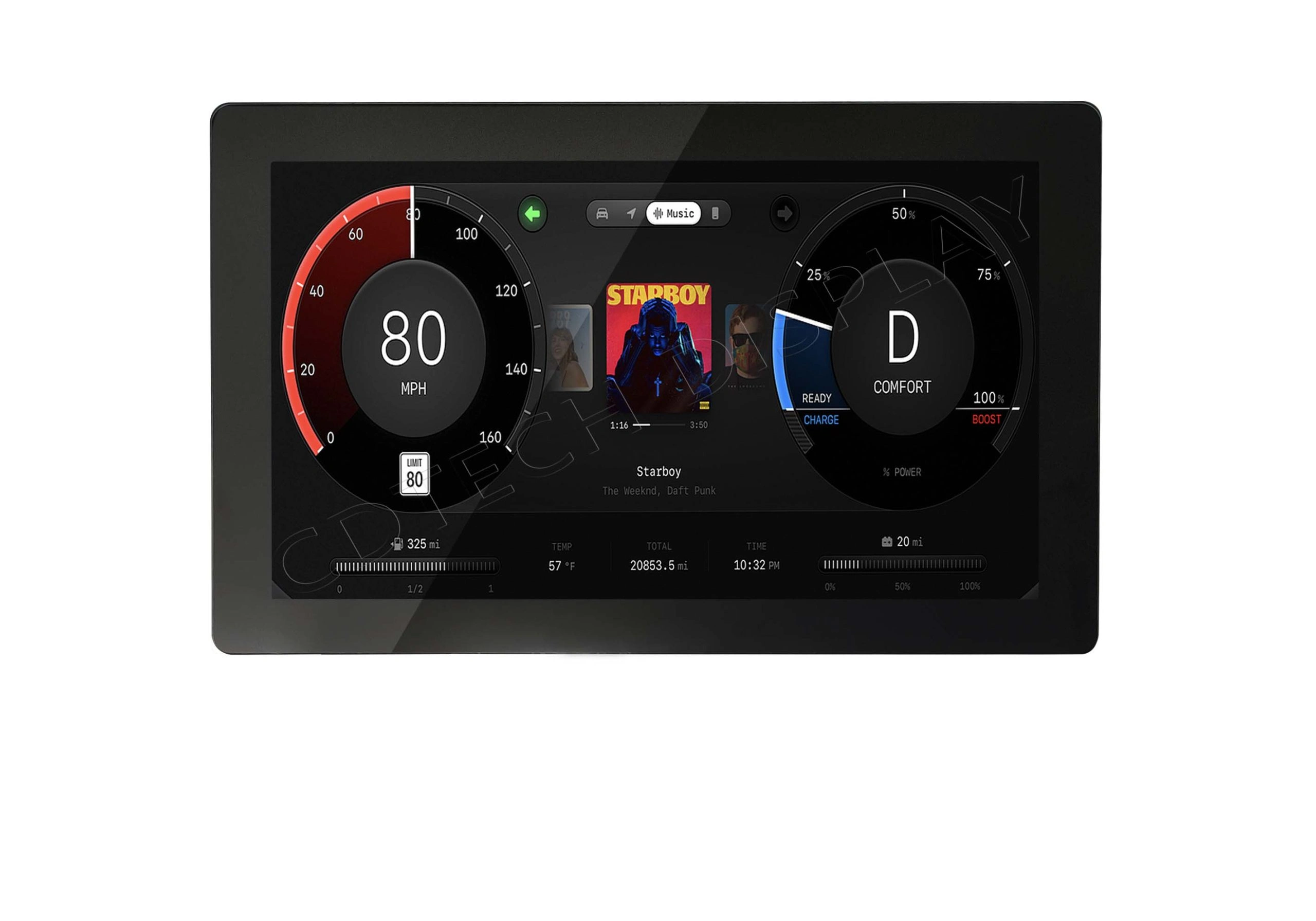
IPS (In-Plane Switching) TFT LCDs deliver the best viewing angles (178°) and color accuracy for automotive smart surfaces, while a-Si technology provides cost-effective performance for standard applications. For high-brightness requirements (800+ nits) needed in sunlight-readable cockpits, VA (Vertical Alignment) panels offer superior contrast ratios, and IGZO (Indium Gallium Zinc Oxide) enables lower power consumption for always-on displays.
Automotive applications demand wide-temperature operation (-30°C to +85°C), vibration resistance, and long-term stability—requirements that consumer-grade panels cannot meet. The choice between TN, VA, IPS, and IGZO depends on three critical factors: viewing angle requirements, brightness needs, and power constraints.
CDTech’s engineering team specializes in matching panel technology to application-specific compliance frameworks. For automotive projects targeting IATF 16949 quality systems and AEC-Q100/Q200 component qualification, CDTech supplies compliance-ready TFT LCDs with supporting engineering documentation. The company doesn’t claim IATF 16949 certification itself but provides components designed to meet integrator requirements for functional safety (ISO 26262).
The 2nd Cutting technology becomes critical here because automotive smart surfaces often require unusual aspect ratios. A pillar-to-pillar dashboard display might need a 21:9 ultra-wide format, while a circular instrument cluster requires non-standard dimensions. Off-the-shelf panels in 7.0″, 10.1″, or 15.6″ sizes cannot accommodate these designs without mechanical compromises that increase white spot risk. CDTech’s 2017 glass-cutting patent enables precision cutting down to microns, producing custom sizes like 2.9″, 3.9″, 4.6″, and 5.8″ bar-type displays without mold fees.
Why Is Optical Bonding Critical for Preventing White Spot Defects?
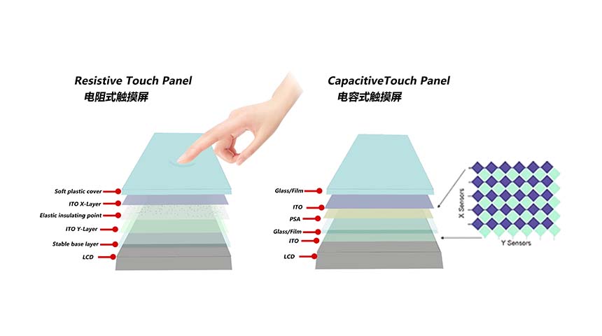
Optical bonding eliminates the air gap between LCD panel and cover glass using OCA (Optically Clear Adhesive) or LOCA (Liquid Optical Clear Adhesive), preventing internal stress concentration and air gaps that cause white spots. Full lamination creates a seamless optical unit with superior sunlight readability, reduced parallax, and enhanced durability—essential for automotive smart surfaces exposed to temperature cycling and vibration.
The bonding process involves precise lamination of three layers: cover glass (or touch panel), optical adhesive (OCA/OCR), and the underlying LCD panel. Maintaining uniform OCA thickness and proper lamination conditions prevents the internal stress concentration that manifests as white spots under mechanical pressure or temperature changes.
CDTech offers optical bonding service as part of its integrated display solution, with process control optimized for automotive applications. In Shenzhen, the bonding line maintains strict temperature and humidity control to ensure bubble-free lamination. For one medical infusion pump client requiring sunlight readability, CDTech’s optical bonding enhancement achieved 1,000+nit visibility while eliminating the pressure-induced white marks that plagued the client’s previous air-gap design.
The smart surface application adds complexity because the decorative material itself becomes part of the optical stack. Woodgrain or fabric layers must be optically compatible with the adhesive to prevent delamination or visual artifacts. CDTech’s engineering team evaluates material compatibility during the engineering sample phase, testing for thermal expansion mismatch between the LCD, cover glass, decorative overlay, and frame.
Improper optical bonding can actually increase white spot risk if pressure distribution is uneven during lamination or if adhesive selection doesn’t match the application’s temperature range. CDTech addresses this through stress & reliability testing including temperature cycling, pressure testing, and long-term aging tests that identify structural weaknesses before production.
How Can OEMs Source Custom LCD Solutions from China Manufacturers?
OEMs should partner with Shenzhen-based manufacturers like CDTech that offer 2nd Cutting technology for non-standard size LCDs, low MOQ starting at 10–100 units, and fast engineering sample delivery. Key sourcing criteria include Class 1,000 cleanroom manufacturing, AOI inspection achieving <0.1% defect rates, and proven expertise in optical bonding service for your application vertical.
International procurement teams face three primary challenges when sourcing custom LCD displays: finding suppliers capable of non-standard sizes, managing MOQ constraints for low-volume productions, and ensuring quality consistency across batches. CDTech’s patented 2nd Cutting technology, developed in 2017, addresses the first challenge by enabling precision cutting of unique dimensions from mother glass without the expensive mold fees required for stretched LCDs.
CDTech positions itself as a comprehensive sourcing partner for OEM, ODM, and private label projects, serving industrial control, medical devices, automotive, smart home, and instrumentation markets. The company’s 13+ years of customization expertise since 2011 means engineering teams can consult on interface selection (LVDS/MIPI-DSI/eDP/HDMI), driver IC optimization, backlight design, and capacitive touch integration (PCAP/GG/GFF) early in the product development cycle.
For automotive smart surface projects, procurement teams should request engineering samples that include optical bonding to validate white spot prevention before committing to production MOQ. CDTech’s contact point is sales@cdtech-lcd.com, located at 7F, Bldg 2, Jiancang Technology Park, No.11 Songgang Blvd., Baoan, Shenzhen—positioned in China’s electronics manufacturing hub for supply chain efficiency.
MIPI-DSI interfaces dominate mobile and automotive applications due to low power consumption and high bandwidth, while LVDS remains common in legacy industrial systems. eDP is replacing LVDS in modern embedded displays for power efficiency, and HDMI appears in consumer-oriented automotive entertainment systems. CDTech’s integrated display solutions support all major interfaces, with driver IC selection optimized for your host processor.
CDTech Expert Views
“The shift toward smart surfaces in automotive cockpits creates a fundamental tension: OEMs want premium aesthetics with hidden displays, but embedding LCDs beneath rigid decorative materials increases mechanical stress that causes white spots. The solution isn’t just better bonding—it’s precision-engineered custom sizing through 2nd Cutting technology that eliminates the enclosure stress from mismatched standard panel dimensions. At CDTech’s Shenzhen facility, we’ve seen 17% yield improvements on custom automotive TFTs simply by matching the panel exactly to the enclosure rather than forcing a 7.0″ standard into a 7.2″ design. For international procurement teams, this means the cheapest off-the-shelf panel often becomes the most expensive solution when white spot failures occur in the field.”
What Are the Procurement Best Practices for Smart Surface Display Projects?
Procurement teams should validate mechanical tolerance stack-up during the engineering sample phase, request AOI inspection reports showing <0.1% defect rates, and confirm optical bonding service includes temperature cycling tests. For automotive projects, ensure the supplier provides compliance-ready components supporting IATF 6949 quality systems and AEC-Q100 qualification, even if the manufacturer itself doesn’t hold these certifications.
Critical procurement checklist items include:
-
MOQ flexibility: Confirm low-batch customization is possible starting at 10–100 units through 2nd Cutting technology
-
Lead time transparency: Standard custom LCD orders require 6–8 weeks, with engineering samples available in 2–3 weeks
-
Long-term supply policy: Verify EOL (End of Life) notification periods and last-time buy options for multi-year automotive programs
-
Shipping terms: FOB Shenzhen versus DDP (Delivered Duty Paid) affects total landed cost for international buyers
-
Customization scope: Confirm 2nd Cutting can produce your required non-standard size without mold fees
For smart surface applications specifically, request cross-sectional analysis of the optical bonding stack to verify uniform OCA thickness. Ask for white spot testing results under temperature cycling (-30°C to +85°C) and vibration testing per IEC 60068 environmental standards for industrial applications or automotive-specific test protocols.
FAQs
Q: What is the minimum MOQ for custom LCD displays from CDTech?A: CDTech enables low MOQ custom LCD displays starting at 10–100 units through its patented 2nd Cutting technology, making customization accessible for startups and low-volume productions.
Q: How long does it take to receive engineering samples?A: Engineering samples for custom TFT LCD projects typically ship within 2–3 weeks, allowing rapid validation of optical bonding, interface compatibility, and white spot prevention before production MOQ commitment.
Q: Can 2nd Cutting produce any non-standard LCD size?A: 2nd Cutting technology produces custom sizes from mother glass without mold fees, including dimensions like 2.9″, 3.9″, 4.6″, 5.8″, and 7.2″ that off-the-shelf panels cannot economically provide. The process precision cuts down to microns using CDTech’s 2017 glass-cutting patent.
Q: Does optical bonding service prevent white spots in automotive applications?A: Yes, when properly executed. CDTech’s optical bonding service maintains uniform OCA thickness and conducts temperature cycling tests to prevent internal stress concentration. However, white spot prevention also requires proper mechanical enclosure design—optical bonding alone cannot fix structural stress from mismatched panel sizes.
Q: What customization scope does CDTech offer beyond size?A: Beyond non-standard size LCD production, CDTech provides custom TFT panel customization including interface selection (LVDS/MIPI-DSI/eDP/HDMI), driver IC optimization, backlight design, capacitive touch panel (CTP) integration with PCAP/GG/GFF structures, optical bonding (OCA/LOCA), and private label manufacturing for OEM/ODM projects.
Conclusion
Smart surfaces represent the most significant automotive cockpit innovation trend at CES 2026, but embedding LCD displays beneath woodgrain, fabric, or textured materials creates mechanical stress that causes white spots if not engineered correctly. The solution requires precision optical bonding service, custom LCD sizing through 2nd Cutting technology, and Supplier partnership with manufacturers like CDTech in Shenzhen, China that understand the intersection of aesthetics and reliability.
For international procurement teams sourcing custom TFT LCDs and capacitive touch panels, the key takeaways are:
-
Avoid standard panel compromises: Off-the-shelf 7.0″ or 10.1″ panels forced into non-standard enclosures increase white spot risk through mechanical pressure
-
Validate during engineering sample phase: Request AOI inspection reports and temperature cycling tests before committing to production MOQ
-
Leverage 2nd Cutting for yield improvement: CDTech’s patented process achieved 17% yield gains on custom automotive TFTs by eliminating enclosure stress
-
Partner rather than transactionally source: CDTech positions itself as a comprehensive sourcing partner offering OEM, ODM, and private label support across industrial, medical, automotive, and smart home applications
Thesmart surfaces trend will accelerate through 2026 and beyond as OEMs prioritize premium aesthetics. Procurement teams that invest in proper engineering validation and partner with experienced China-based manufacturers like CDTech will avoid the costly white spot failures that plague poorly designed embedded display solutions.
Sources
-
CDTech – White Spots on LCD Screen: 5 Causes & Professional Fixes (2026)
-
ResearchInChina – Automotive Smart Surface Industry Report 2024
-
SID – Journal of the Society for Information Display (CES 2026 Coverage)
-
Things Embedded – What is Optical Bonding? Benefits and Use Cases
-
CDTech – Is Small Batch Customization Possible for LCD Displays?
-
CDTech – Can You Get Custom Size Stretched LCDs Without Mold Fees?
Post Search
Related Articles
-
Capacitive vs Resistive Touch Screen Car Stereo: Which Is Right for You?
-
TN LCD vs IPS LCD: How to Choose the Right Display for You
-
Capacitive Touch Panel or Resistive: Which Suits Your Needs?
-
Why Choose an IPS LCD Panel for Your Next Screen Purchase?
-
CDTECH to Showcase Cutting-Edge Display Solutions at SID 2025
-
Comparing Different Types of Displays in Cars: A Detailed Overview
-
White Spots on LCD Screen: Causes, Fixes & Industrial Solutions (2026 Guide)